SNVSBK9G November   2019  – November 2024 LM63635-Q1

PRODUCTION DATA  

  1.   1
  2. Features
  3. Applications
  4. Description
  5. Device Comparison Table
  6. Pin Configuration and Functions
  7. Specifications
    1. 6.1 Absolute Maximum Ratings
    2. 6.2 ESD Ratings
    3. 6.3 Recommended Operating Conditions
    4. 6.4 Thermal Information
    5. 6.5 Electrical Characteristics
    6. 6.6 Timing Characteristics
    7. 6.7 Switching Characteristics
    8. 6.8 System Characteristics
    9. 6.9 Typical Characteristics
  8. Detailed Description
    1. 7.1 Overview
    2. 7.2 Functional Block Diagram
    3. 7.3 Feature Description
      1. 7.3.1 Sync/Mode Selection
      2. 7.3.2 Output Voltage Selection
      3. 7.3.3 Switching Frequency Selection
        1. 7.3.3.1 Spread Spectrum Option
      4. 7.3.4 Enable and Start-Up
      5. 7.3.5 RESET Flag Output
      6. 7.3.6 Undervoltage Lockout and Thermal Shutdown and Output Discharge
    4. 7.4 Device Functional Modes
      1. 7.4.1 Overview
      2. 7.4.2 Light Load Operation
        1. 7.4.2.1 Sync/FPWM Operation
      3. 7.4.3 Dropout Operation
      4. 7.4.4 Minimum On-time Operation
      5. 7.4.5 Current Limit and Short-Circuit Operation
  9. Application and Implementation
    1. 8.1 Application Information
    2. 8.2 Typical Application
      1. 8.2.1 Design Requirements
      2. 8.2.2 Detailed Design Procedure
        1. 8.2.2.1 Choosing the Switching Frequency
        2. 8.2.2.2 Setting the Output Voltage
          1. 8.2.2.2.1 CFF Selection
        3. 8.2.2.3 Inductor Selection
        4. 8.2.2.4 Output Capacitor Selection
        5. 8.2.2.5 Input Capacitor Selection
        6. 8.2.2.6 CBOOT
        7. 8.2.2.7 VCC
        8. 8.2.2.8 External UVLO
        9. 8.2.2.9 Maximum Ambient Temperature
      3. 8.2.3 Full Feature Design Example
      4. 8.2.4 Application Curves
      5. 8.2.5 EMI Performance Curves
    3. 8.3 Best Design Practices
    4. 8.4 Power Supply Recommendations
    5. 8.5 Layout
      1. 8.5.1 Layout Guidelines
        1. 8.5.1.1 Ground and Thermal Considerations
      2. 8.5.2 Layout Example
  10. Device and Documentation Support
    1. 9.1 Device Support
      1. 9.1.1 Device Nomenclature
    2. 9.2 Documentation Support
      1. 9.2.1 Related Documentation
    3. 9.3 Receiving Notification of Documentation Updates
    4. 9.4 Support Resources
    5. 9.5 Trademarks
    6. 9.6 Electrostatic Discharge Caution
    7. 9.7 Glossary
  11. 10Revision History
  12. 11Mechanical, Packaging, and Orderable Information

Description

The LM63635-Q1 regulator is an easy-to-use, synchronous, step-down DC/DC converter designed for rugged automotive applications. The LM63635-Q1 can drive up to 3.25A of load current from an input of up to 36V for WSON package and 32V for HTSSOP package. The converter has high light load efficiency and output accuracy in a small design size. Features such as a RESET flag and precision enable provide both flexible and easy-to-use solutions for a wide range of applications. Automatic frequency foldback at light load improves efficiency while maintaining tight load regulation. Integration eliminates many external components and provides a pinout designed for simple PCB layout. Protection features include thermal shutdown, input undervoltage lockout, cycle-by-cycle current limit, and hiccup short-circuit protection. The LM63635-Q1 is available in both the HTSSOP 16-pin power package, with PowerPAD™ integrated circuit package, and the WSON 12-pin power package.

Package Information
PART NUMBER PACKAGE(1) PACKAGE SIZE(2)
LM63635-Q1 PWP (HTSSOP, 16) 6.40mm × 5.00mm
DRR (WSON, 12) 3.00mm × 3.00mm
For more information, see Section 11.
The package size (length × width) is a nominal value and includes pins, where applicable
LM63635-Q1 Simplified SchematicSimplified Schematic
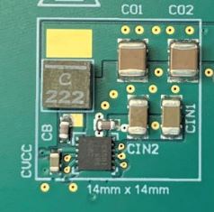
LM63635-Q1 Typical Design Example IOUT =
                        3.25A, ƒSW = 2200kHzTypical Design Example IOUT = 3.25A,
ƒSW = 2200kHz