-
LMQ644xx-Q1 3V to 36V, Low IQ, Dual 6/5/4A, Automotive Buck Converter Optimized for Power Density and Low EMI SNVSC42A September 2023 – July 2024 LMQ64480-Q1 , LMQ644A0-Q1 , LMQ644A2-Q1
PRODUCTION DATA
-
LMQ644xx-Q1 3V to 36V, Low IQ, Dual 6/5/4A, Automotive Buck Converter Optimized for Power Density and Low EMI
- 1
- 1 Features
- 2 Applications
- 3 Description
- 4 Device Comparison Table
- 5 Pin Configuration and Functions
- 6 Specifications
-
7 Detailed Description
- 7.1 Overview
- 7.2 Functional Block Diagram
- 7.3
Feature Description
- 7.3.1 Input Voltage Range (VIN)
- 7.3.2 Enable EN Pin and Use as VIN UVLO
- 7.3.3 Output Voltage Selection and Soft Start
- 7.3.4 SYNC Allows Clock Synchronization and Mode Selection
- 7.3.5 Clock Locking
- 7.3.6 Adjustable Switching Frequency
- 7.3.7 Power-Good Output Voltage Monitoring
- 7.3.8 Internal LDO, VCC UVLO, and BIAS Input
- 7.3.9 Bootstrap Voltage and VCBOOT-UVLO (CB1 and CB2 Pin)
- 7.3.10 CONFIG Device Configuration Pin
- 7.3.11 Spread Spectrum
- 7.3.12 Soft Start and Recovery From Dropout
- 7.3.13 Overcurrent and Short-Circuit Protection
- 7.3.14 Hiccup
- 7.3.15 Thermal Shutdown
- 7.4 Device Functional Modes
-
8 Application and Implementation
- 8.1 Application Information
- 8.2
Typical Application
- 8.2.1 Design Requirements
- 8.2.2
Detailed Design Procedure
- 8.2.2.1 Choosing the Switching Frequency
- 8.2.2.2 Setting the Output Voltage
- 8.2.2.3 Inductor Selection
- 8.2.2.4 Output Capacitor Selection
- 8.2.2.5 Input Capacitor Selection
- 8.2.2.6 BOOT Capacitor
- 8.2.2.7 VCC
- 8.2.2.8 CFF and RFF Selection
- 8.2.2.9 SYNCHRONIZATION AND MODE
- 8.2.2.10 External UVLO
- 8.2.2.11 Typical Thermal Performance
- 8.2.3 Application Curves
- 8.3 Power Supply Recommendations
- 8.4 Layout
- 9 Device and Documentation Support
- 10Revision History
- 11Mechanical, Packaging, and Orderable Information
- IMPORTANT NOTICE
LMQ644xx-Q1 3V to 36V, Low IQ, Dual 6/5/4A, Automotive Buck Converter Optimized for Power Density and Low EMI
1 Features
- AEC-Q100 qualified for automotive applications:
- Device temperature grade 1: –40°C to +125°C ambient operating temperature
- Operation up to 150°C junction temperature
- Functional Safety-Capable
- Designed for Low EMI
- Symmetrical input voltage pins with > 1mm clearance to ground
- Four 22nF integrated VIN
to GND bypass capacitors
- Two bypass capacitors placed in series between each VIN and GND for high reliability
- Pin selectable spread spectrum option
- Pin selectable FPWM or auto mode operation
- Enhanced HotRod™ QFN (25) package with wettable flanks
- Switching frequency from 100kHz to 2.2MHz
- Meets CISPR 25 class 5 EMI requirements
- Single and dual-output features
- Wide input voltage range of 3V to 36V
- 1% accurate fixed 3.3V, 5V or adjustable outputs from 0.8V to 20V
- Hiccup-mode overcurrent protection and thermal shutdown protection with hysteresis
- Precision ENABLE and PGOOD functions
- 50ns tON(min) for high VIN / VOUT ratio
- 80ns tOFF(min) for low dropout
- Versatile dual-output operation
- Shutdown mode current: 0.5µA typical
- No-load standby current: 9µA typical
- Built-in compensation and 3ms soft start
- Independent precision ENABLE and PGOOD
- Adaptable single-output operation
- > 95% efficient for an 8A load, single output, VIN =12V, VOUT = 5V
- External compensation and adjustable soft start
- PGOOD, SYNCIN, and SYNCOUT functions
2 Applications
- Automotive infotainment and cluster: head unit, media hub, USB charge, display
- Automotive ADAS and body electronics
- General-purpose dual buck converters
3 Description
The LMQ644xx-Q1 is a 36V, synchronous, buck, DC/DC converter for high-current single or dual outputs. The device uses an interleaved, stackable, current-mode control architecture for easy loop compensation, fast transient response, excellent load and line regulation, and accurate current sharing with an output clock supporting up to 6 phases for currents up to 36A. A high-side switch minimum on-time of 50ns gives large step-down ratios, enabling the direct conversion from 12V, 24V, or automotive inputs to low-voltage rails for reduced system complexity and design cost.
The LMQ644xx-Q1 incorporates spread spectrum in an optimized enhanced HotRod QFN package, with wettable flanks, and four 22nF high frequency integrated capacitors to minimize EMI. Dual Random Spread Spectrum (DRSS) frequency hopping is set to ±10% (typical), drastically reducing emissions through a combination of triangular and pseudo-random modulation. A bias pin allows the LMQ644xx-Q1 to save losses by powering the device from the output of the converter, achieving a 9μA no-load quiescent current to extend the operating run-time in battery-powered systems. The LMQ644xx-Q1 can maintain high efficiency light-load operation even when stacking multiple devices for high efficiency over the full load range.
| PART NUMBER(2) | PACKAGE(1) | BODY SIZE (NOM) |
|---|---|---|
| LMQ644A2-Q1 | RXA (VQFN-FCRLF, 24) | 4.0mm × 5.0mm |
| LMQ644A0-Q1 | ||
| LMQ64480-Q1 |
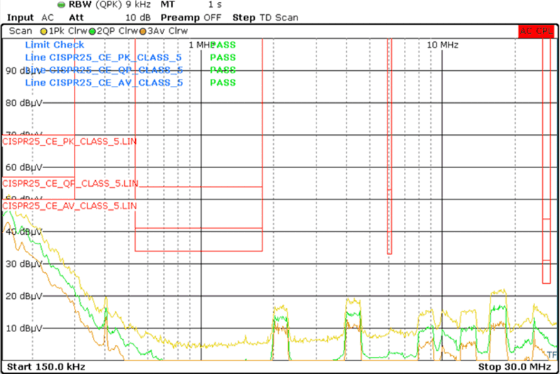
 CISPR 25
Conducted, VOUT = 3.3V, 2.1MHz, 12A