SNVSC42A September 2023 – July 2024 LMQ64480-Q1 , LMQ644A0-Q1 , LMQ644A2-Q1
PRODUCTION DATA
- 1
- 1 Features
- 2 Applications
- 3 Description
- 4 Device Comparison Table
- 5 Pin Configuration and Functions
- 6 Specifications
-
7 Detailed Description
- 7.1 Overview
- 7.2 Functional Block Diagram
- 7.3
Feature Description
- 7.3.1 Input Voltage Range (VIN)
- 7.3.2 Enable EN Pin and Use as VIN UVLO
- 7.3.3 Output Voltage Selection and Soft Start
- 7.3.4 SYNC Allows Clock Synchronization and Mode Selection
- 7.3.5 Clock Locking
- 7.3.6 Adjustable Switching Frequency
- 7.3.7 Power-Good Output Voltage Monitoring
- 7.3.8 Internal LDO, VCC UVLO, and BIAS Input
- 7.3.9 Bootstrap Voltage and VCBOOT-UVLO (CB1 and CB2 Pin)
- 7.3.10 CONFIG Device Configuration Pin
- 7.3.11 Spread Spectrum
- 7.3.12 Soft Start and Recovery From Dropout
- 7.3.13 Overcurrent and Short-Circuit Protection
- 7.3.14 Hiccup
- 7.3.15 Thermal Shutdown
- 7.4 Device Functional Modes
-
8 Application and Implementation
- 8.1 Application Information
- 8.2
Typical Application
- 8.2.1 Design Requirements
- 8.2.2
Detailed Design Procedure
- 8.2.2.1 Choosing the Switching Frequency
- 8.2.2.2 Setting the Output Voltage
- 8.2.2.3 Inductor Selection
- 8.2.2.4 Output Capacitor Selection
- 8.2.2.5 Input Capacitor Selection
- 8.2.2.6 BOOT Capacitor
- 8.2.2.7 VCC
- 8.2.2.8 CFF and RFF Selection
- 8.2.2.9 SYNCHRONIZATION AND MODE
- 8.2.2.10 External UVLO
- 8.2.2.11 Typical Thermal Performance
- 8.2.3 Application Curves
- 8.3 Power Supply Recommendations
- 8.4 Layout
- 9 Device and Documentation Support
- 10Revision History
- 11Mechanical, Packaging, and Orderable Information
7.3.2 Enable EN Pin and Use as VIN UVLO
Apply a voltage less than 0.25 V to the EN1 pin to put the LMQ644xx into shutdown mode. In shutdown mode, the quiescent current drops to 0.5 µA (typical). Above this voltage but below the lower EN threshold, VCC is active but switching on SW1 and SW2 remains inactive. After EN1 is above VEN, the SW1 becomes active. EN2 controls switching on the second output SW2. In dual output configuration EN2 can be used to independantly turn off the second output voltage, but does not control entering shutdown mode. In single-output multi-phase configuration EN1 on primaries and secondaries must be tied together. In single output configuration EN1 must not be used to disable the secondary devices for phase shedding. EN2 of the primary and secondaries must be tied together and can be used to shutdown the secondary phases. The very high efficiency of the device in PFM operation eliminates the need to phase shed in most designs as phase of the secondaries is controlled even under PFM operation.
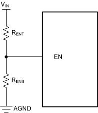
The EN terminals cannot be left floating. The simplest way to enable the operation is to connect the EN pins to VIN. This action allows the self-start-up of the device when VIN drives the internal VCC above its UVLO level. However, many applications benefit from employing an enable divider string, which establishes a precision input undervoltage lockout (UVLO). The precision UVLO can be used for the following:
- Sequencing
- Preventing the device from retriggering when used with long input cables
- Reducing the occurrence of deep discharge of a battery power source
 Figure 7-2 VIN UVLO Using the EN Pin
Resistor values can be calculated using the equation below:
where
- VON = VIN turn-on voltage
- VOFF = VIN turn-off voltage