SNVSC42A September 2023 – July 2024 LMQ64480-Q1 , LMQ644A0-Q1 , LMQ644A2-Q1
PRODUCTION DATA
- 1
- 1 Features
- 2 Applications
- 3 Description
- 4 Device Comparison Table
- 5 Pin Configuration and Functions
- 6 Specifications
-
7 Detailed Description
- 7.1 Overview
- 7.2 Functional Block Diagram
- 7.3
Feature Description
- 7.3.1 Input Voltage Range (VIN)
- 7.3.2 Enable EN Pin and Use as VIN UVLO
- 7.3.3 Output Voltage Selection and Soft Start
- 7.3.4 SYNC Allows Clock Synchronization and Mode Selection
- 7.3.5 Clock Locking
- 7.3.6 Adjustable Switching Frequency
- 7.3.7 Power-Good Output Voltage Monitoring
- 7.3.8 Internal LDO, VCC UVLO, and BIAS Input
- 7.3.9 Bootstrap Voltage and VCBOOT-UVLO (CB1 and CB2 Pin)
- 7.3.10 CONFIG Device Configuration Pin
- 7.3.11 Spread Spectrum
- 7.3.12 Soft Start and Recovery From Dropout
- 7.3.13 Overcurrent and Short-Circuit Protection
- 7.3.14 Hiccup
- 7.3.15 Thermal Shutdown
- 7.4 Device Functional Modes
-
8 Application and Implementation
- 8.1 Application Information
- 8.2
Typical Application
- 8.2.1 Design Requirements
- 8.2.2
Detailed Design Procedure
- 8.2.2.1 Choosing the Switching Frequency
- 8.2.2.2 Setting the Output Voltage
- 8.2.2.3 Inductor Selection
- 8.2.2.4 Output Capacitor Selection
- 8.2.2.5 Input Capacitor Selection
- 8.2.2.6 BOOT Capacitor
- 8.2.2.7 VCC
- 8.2.2.8 CFF and RFF Selection
- 8.2.2.9 SYNCHRONIZATION AND MODE
- 8.2.2.10 External UVLO
- 8.2.2.11 Typical Thermal Performance
- 8.2.3 Application Curves
- 8.3 Power Supply Recommendations
- 8.4 Layout
- 9 Device and Documentation Support
- 10Revision History
- 11Mechanical, Packaging, and Orderable Information
7.3.3 Output Voltage Selection and Soft Start
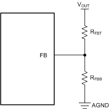
A voltage divider between the output voltage and the FB1 pin is used to create an adjustable output voltage from 0.8 to 20 V for the first buck converter. The thevenin impedance of the divider must be larger than 4 kohms, to correctly enter adjustable output voltage configuration. For lower output voltages a minimum of 10 kohms is recommended for RFBT to meet this requirement. For a fixed 5-V output connect FB1 to VCC through a 10 kohm resistor. For a fixed 3.3 V connect FB1 to AGND. For fixed output voltage configurations the first channel output voltage is sensed on pin 13 BIAS/VOSNS1.
For dual-output voltage configuration, RCONFIG = 0 (spread spectrum disabled) or 121 kΩ (spread spectrum enabled).
FB2 is configured in the same manner as FB1. A voltage divider between output voltage and the FB2 pin is used to create an adjustable output voltage from 0.8 to 20 V for the second buck converter. The thevenin impedance of the divider must be larger than 4 kohms, to correctly enter adjustable output voltage configuration. For lower output voltages a value of 10 kohms is recommended for RFBT to meet this requirement. For a fixed 5-V output, connect FB2 to VCC through a 10 kohm resistor. For a fixed 3.3 V connect FB2 to AGND. For fixed output voltage configurations, the second channel output voltage is sensed on pin 19. that is, VOSNS2.
Current sharing between multiple buck channels can increase the current. For one device, single-output multi-phase operation can double the single buck current and provide up to 12 A. Using three devices allows six times the current up to 36 A. When the device is configured to single-output multi-phase operation (9.53 kΩ < RCONFIG < 93.1kΩ) , FB2 is re-configured to provide an adjustable soft start (SS). An external capacitor can be placed from this pin to ground to extend the internal soft-start time. The time can be calculated using the soft-start current of 20 µA (typical) charging the external capacitor to the reference voltage of 0.8 V (typical). As an example, a 220-nF capacitor provides a soft start of 8 ms after the initialization of the device. The pin must also be tied to FB2/SS of all other LMQ stacked devices for fault communication between primary and secondary devices. Faults, such as thermal shutdown, are communicated by pulling the pin low and stops switching for all devices.
 Figure 7-3 Setting Output
Voltage of Adjustable Versions
Figure 7-3 Setting Output
Voltage of Adjustable VersionsThe LMQ644xx uses a 0.8-V reference. The following equation can be used to determine RFBB for a desired output voltage and a given RFBT. Usually, RFBT is limited to a maximum value of 100 kΩ to prevent drifting due to PCB leakage under harsh conditions. To improve light load efficiency, a larger resistance of up to 1 MΩ can be used in cleaner environments, or the fixed output voltage options can be used under harsher conditions.
In addition, a feedforward capacitor CFF can be used to optimize the transient response. Typical values are provided in the applications section and were selected based upon the top feedback resistor to place a zero slightly above the cross-over frequency.