SNVSCG7 November 2024 LM5190
PRODUCTION DATA
- 1
- 1 Features
- 2 Applications
- 3 Description
- 4 Pin Configuration and Functions
- 5 Specifications
-
6 Detailed Description
- 6.1 Overview
- 6.2 Functional Block Diagram
- 6.3
Feature Description
- 6.3.1 Input Voltage Range (VIN)
- 6.3.2 High-Voltage Bias Supply Regulator (VCC, BIAS)
- 6.3.3 Precision Enable (EN)
- 6.3.4 Power-Good Monitor (PGOOD)
- 6.3.5 Switching Frequency (RT)
- 6.3.6 Low Dropout Mode
- 6.3.7 Dual Random Spread Spectrum (DRSS)
- 6.3.8 Soft Start
- 6.3.9 Output Voltage Setpoint (FB)
- 6.3.10 Minimum Controllable On Time
- 6.3.11 Inductor Current Sense (ISNS+, VOUT)
- 6.3.12 Voltage Loop Error Amplifier
- 6.3.13 Current Monitor, Programmable Current Limit, and Current Loop Error Amplifier (IMON/ILIM, ISET)
- 6.3.14 Dual Loop Architecture
- 6.3.15 PWM Comparator
- 6.3.16 Slope Compensation
- 6.3.17 Hiccup Mode Current Limiting
- 6.3.18 High-Side and Low-Side Gate Drivers (HO, LO)
- 6.4 Device Functional Modes
- 7 Application and Implementation
- 8 Device and Documentation Support
- 9 Revision History
- 10Mechanical, Packaging, and Orderable Information
6.3.7 Dual Random Spread Spectrum (DRSS)
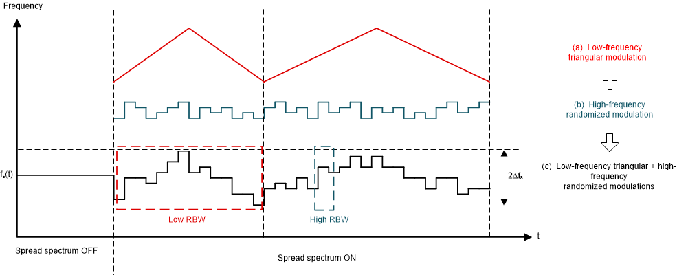
The LM5190 provides a digital spread spectrum, which reduces the EMI of the power supply over a wide frequency range. DRSS combines a low-frequency triangular modulation profile with a high frequency cycle-by-cycle random modulation profile. The low-frequency triangular modulation improves performance in lower radio-frequency bands, while the high-frequency random modulation improves performance in higher radio frequency bands.
Spread spectrum works by converting a narrowband signal into a wideband signal that spreads the energy over multiple frequencies. Because industry standards require different EMI receiver resolution bandwidth (RBW) settings for different frequency bands, the RBW has an impact on the spread spectrum performance. . DRSS is able to simultaneously improve the EMI performance in the low and high RBWs using the low-frequency triangular modulation profile and at high frequency cycle-by-cycle random modulation, respectively. DRSS can reduce conducted emissions up to 15dBμV in the low-frequency band (150kHz to 30MHz) and 5dBμV in the high-frequency band (30MHz to 108MHz).
To enable DRSS, connect RT to VCC through a resistor during initial power on. The resistor is still used to set the switching frequency with the same equation in Equation 1.
 Figure 6-2 Dual Random Spread Spectrum Implementation