SNVSCI9A June 2024 – September 2024 LMR36503E-Q1
PRODUCTION DATA
- 1
- 1 Features
- 2 Applications
- 3 Description
- 4 Device Comparison Table
- 5 Pin Configuration and Functions
- 6 Specifications
-
7 Detailed Description
- 7.1 Overview
- 7.2 Functional Block Diagram
- 7.3
Feature Description
- 7.3.1 Enable, Start-Up, and Shutdown
- 7.3.2 External CLK SYNC (with MODE/SYNC)
- 7.3.3 Adjustable Switching Frequency (with RT)
- 7.3.4 Power-Good Output Operation
- 7.3.5 Internal LDO, VCC UVLO, and VOUT/BIAS Input
- 7.3.6 Bootstrap Voltage and VCBOOT-UVLO (CBOOT Terminal)
- 7.3.7 Output Voltage Selection
- 7.3.8 Soft Start and Recovery from Dropout
- 7.3.9 Current Limit and Short Circuit
- 7.3.10 Thermal Shutdown
- 7.3.11 Input Supply Current
- 7.4 Device Functional Modes
-
8 Application and Implementation
- 8.1 Application Information
- 8.2
Typical Application
- 8.2.1 Design Requirements
- 8.2.2 Detailed Design Procedure
- 8.2.3 Application Curves
- 8.3 Best Design Practices
- 8.4 Power Supply Recommendations
- 8.5 Layout
- 9 Device and Documentation Support
- 10Revision History
- 11Mechanical, Packaging, and Orderable Information
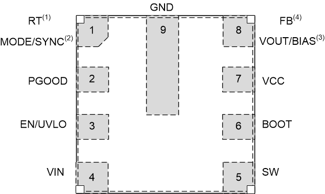
5 Pin Configuration and Functions

A. See Section 4 for more details. Pin 1 trimmed and factory-set for externally adjustable
switching frequency RT variants only.
B. Pin 1 factory-set for fixed switching
frequency MODE/SYNC variants only.
C. Pin 8 trimmed and factory-set for fixed
output voltage VOUT/BIAS variants only.
D. Pin 8 factory-set for adjustable output
voltage FB variants only.
Figure 5-1 9-Pin (2mm × 2mm) VQFN-HR RPE Package (Top
View)Table 5-1 Pin Functions
| PIN | TYPE | DESCRIPTION | ||
|---|---|---|---|---|
| NO. | NAME | |||
| 1 | RT or MODE/SYNC |
A | When the device is trimmed as the RT variant, the
switching frequency can be adjusted from 200kHz to
2.2MHz.When the device is trimmed as the MODE/SYNC
variant, the device can operate in user-selectable
PFM/FPWM mode and can be synchronized to an
external clock. Do not float this pin. |
|
| 2 | PGOOD | A | Open-drain power-good flag output. Connect to a suitable voltage supply through a current limiting resistor. High = power OK, low = power bad. This pin goes low when EN = low. This pin can be open or grounded when not used. | |
| 3 | EN/UVLO | A | Enable input to regulator. High = ON, low = OFF. Can be connected directly to VIN. Do not float this pin. | |
| 4 | VIN | P | Input supply to regulator. Connect a high-quality bypass capacitor or capacitors directly to this pin and GND. | |
| 5 | SW | P | Regulator switch node. Connect to power inductor. | |
| 6 | BOOT | P | Bootstrap supply voltage for internal high-side driver. Connect a high-quality, 100nF capacitor from this pin to the SW pin. | |
| 7 | VCC | P | Internal LDO output. Used as supply to internal control circuits. Do not connect to external loads. Can be used as logic supply for power-good flag. Connect a high-quality, 1µF capacitor from this pin to GND. | |
| 8 | VOUT/BIAS or FB | A | Fixed output options are available with the
VOUT/BIAS pin variant. Connect to output voltage
node for fixed VOUT. Check Section 4 for more details. The FB pin variant can help adjust the output voltage. Connect to tap point of feedback voltage divider. Do not float this pin. |
|
| 9 | GND | G | Power ground terminal. Connect to system ground. Connect to CIN with short, wide traces. | |
| A = Analog, P = Power, G = Ground | ||||