SNVSCI9A June 2024 – September 2024 LMR36503E-Q1
PRODUCTION DATA
- 1
- 1 Features
- 2 Applications
- 3 Description
- 4 Device Comparison Table
- 5 Pin Configuration and Functions
- 6 Specifications
-
7 Detailed Description
- 7.1 Overview
- 7.2 Functional Block Diagram
- 7.3
Feature Description
- 7.3.1 Enable, Start-Up, and Shutdown
- 7.3.2 External CLK SYNC (with MODE/SYNC)
- 7.3.3 Adjustable Switching Frequency (with RT)
- 7.3.4 Power-Good Output Operation
- 7.3.5 Internal LDO, VCC UVLO, and VOUT/BIAS Input
- 7.3.6 Bootstrap Voltage and VCBOOT-UVLO (CBOOT Terminal)
- 7.3.7 Output Voltage Selection
- 7.3.8 Soft Start and Recovery from Dropout
- 7.3.9 Current Limit and Short Circuit
- 7.3.10 Thermal Shutdown
- 7.3.11 Input Supply Current
- 7.4 Device Functional Modes
-
8 Application and Implementation
- 8.1 Application Information
- 8.2
Typical Application
- 8.2.1 Design Requirements
- 8.2.2 Detailed Design Procedure
- 8.2.3 Application Curves
- 8.3 Best Design Practices
- 8.4 Power Supply Recommendations
- 8.5 Layout
- 9 Device and Documentation Support
- 10Revision History
- 11Mechanical, Packaging, and Orderable Information
3 Description
The LMR36503E-Q1 is a 65V, 0.3A synchronous step-down DC/DC converter in 2mm × 2mm HotRod package. This easy-to-use converter can handle input voltage transients up to 70V, provide excellent EMI performance, and support fixed 3.3V, 5V and other adjustable output voltages.
The LMR36503E-Q1 uses peak current mode control architecture with internal compensation and maintains stable operation with minimal output capacitance. The wide input operating range of the LMR36503E-Q1 helps the device remain functional during a deep input voltage sag condition, making the device an excellent choice for automotive applications withstanding severe cold crank start impulses. The PGOOD flag in the LMR36503E-Q1 provides precise indication of the output voltage status, eliminating the requirement for an external supervisor. A seamless transition from FPWM to PFM, with an ultra-low standby quiescent current allows the LMR36503E-Q1 to support much higher system efficiency at low output loads. The MODE/SYNC pin variant helps to synchronize the LMR36503E-Q1 to an external clock. With the right resistor selection, the LMR36503E-Q1 RT pin variant can also be externally programmed to any desired switching frequency of operation. The rich feature set of the LMR36503E-Q1 is designed to simplify implementation for a wide range of automotive end equipments.
 Simplified Schematic
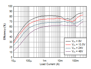
 Efficiency
versus Output Current VOUT = 3.3V (Fixed), 2.2MHz