SNVSCU2A August 2024 – August 2024 LM5137-Q1
ADVANCE INFORMATION
- 1
- 1 Features
- 2 Applications
- 3 Description
- 4 Device Comparison Table
- 5 Pin Configuration and Functions
- 6 Specifications
-
7 Detailed Description
- 7.1 Overview
- 7.2 Functional Block Diagram
- 7.3
Feature Description
- 7.3.1 Input Voltage Range (VIN)
- 7.3.2 Bias Supply Regulator (VCC, BIAS1/VOUT1, VDDA)
- 7.3.3 Precision Enable (EN1, EN2)
- 7.3.4 Switching Frequency (RT)
- 7.3.5 Pulse Frequency Modulation and Synchronization (PFM/SYNC)
- 7.3.6 Synchronization Out (SYNCOUT)
- 7.3.7 Dual Random Spread Spectrum (DRSS)
- 7.3.8 Configurable Soft Start (RSS)
- 7.3.9 Output Voltage Setpoints (FB1, FB2)
- 7.3.10 Minimum Controllable On-Time
- 7.3.11 Error Amplifier and PWM Comparator (FB1, FB2, COMP1, COMP2)
- 7.3.12 Inductor Current Sense (ISNS1+, BIAS1/VOUT1, ISNS2+, VOUT2)
- 7.3.13 MOSFET Gate Drivers (HO1, HO2, LO1, LO2)
- 7.3.14 Output Configurations (CNFG)
- 7.4 Device Functional Modes
-
8 Application and Implementation
- 8.1 Application Information
- 8.2
Typical Applications
- 8.2.1
Design 1 – Dual 5V and 3.3V, 20A Buck Regulator for 12V
Automotive Battery Applications
- 8.2.1.1 Design Requirements
- 8.2.1.2
Detailed Design Procedure
- 8.2.1.2.1 Custom Design With WEBENCH® Tools
- 8.2.1.2.2 Custom Design With Excel Quickstart Tool
- 8.2.1.2.3 Inductor Calculations
- 8.2.1.2.4 Shunt Resistors
- 8.2.1.2.5 Ceramic Output Capacitors
- 8.2.1.2.6 Ceramic Input Capacitors
- 8.2.1.2.7 Feedback Resistors
- 8.2.1.2.8 Input Voltage UVLO Resistors
- 8.2.1.2.9 Compensation Components
- 8.2.1.3 Application Curves
- 8.2.2 Design 2 – Two-Phase, Single-Output Buck Regulator for Automotive ADAS Applications
- 8.2.3 Design 3 – 12V, 20A, 400kHz, Two-Phase Buck Regulator for 48V Automotive Applications
- 8.2.1
Design 1 – Dual 5V and 3.3V, 20A Buck Regulator for 12V
Automotive Battery Applications
- 8.3 Power Supply Recommendations
- 8.4 Layout
- 9 Device and Documentation Support
- 10Revision History
- 11Mechanical, Packaging, and Orderable Information
8.4.1 Layout Guidelines
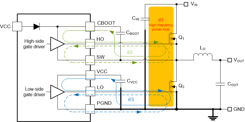
Proper PCB design and layout is important in a high-current, fast-switching circuit (with high current and voltage slew rates) to achieve a robust and reliable design. As expected, certain issues must be considered before designing a PCB layout using the LM5137-Q1. The high-frequency power loop of a buck regulator power stage is denoted by loop 1 in the shaded area of Figure 8-25. The topological architecture of a buck regulator means that particularly high di/dt current flows in the components of loop 1, and reducing the parasitic inductance of this loop by minimizing the effective loop area becomes mandatory. Also important are the gate drive loops of the high-side and low-side MOSFETs, denoted by 2 and 3, respectively, in Figure 8-25.
 Figure 8-25 DC/DC Regulator Ground System With Power Stage and Gate Drive Circuit Switching Loops