SNVU570B December 2017 – February 2022 TPSM846C24
2 Getting Started
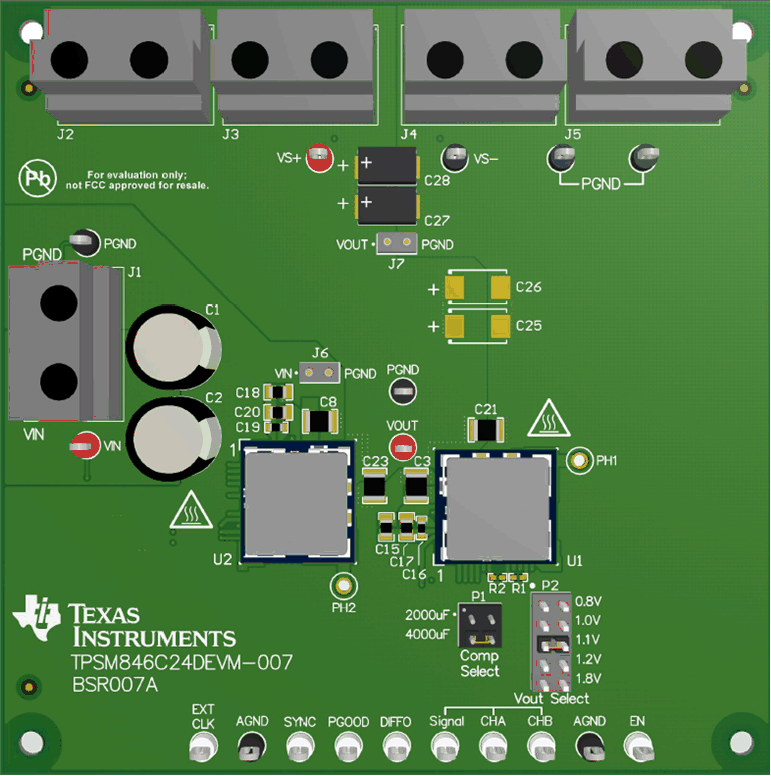
Figure 2-1 highlights the user interface items associated with the EVM. The polarized input power terminal block (TB1) is used for connection to the host input supply. TB2 and TB3 allow four terminals for VOUT and TB4 and TB5 allow four terminals for PGND for connection to the load. These terminal blocks can except up to 12-AWG wire.
 Figure 2-1 EVM User Interface
The VIN monitor (VIN and PGND) and VOUT monitor (VS+ and VS–) test points located near the input terminal block and the output terminal blocks are intended to be used as voltage monitoring points where voltmeters can be connected to measure the input and output voltages. Do not use these VIN and VOUT monitoring test points as the input supply or output load connection points. The PCB traces connecting to these test points are not designed to support high currents.
The VIN scope (J1) and VOUT scope (J2) test points can be used to monitor VIN and VOUT waveforms with an oscilloscope. These test points are intended for use with un-hooded scope probes outfitted with a low-inductance ground lead (ground spring) mounted to the scope barrel. The two sockets of each test point are on 0.1-inch centers. Insert the scope probe tip into the socket labeled VIN or VOUT, and insert the scope ground lead into the hole of the socket labeled PGND.
The test points located directly below the device are made available to test the features of the device. Any external connections made to these test points should be referenced to one of the AGND test points located along the bottom of the EVM. Refer to Section 3 for more information on the individual control test points.
The Vout Select jumper (P4) is used to set the output voltage. The default loading is the 1.0-V position.
The Comp Select jumper (P2) sets the proper frequency compensation for the total amount of output capacitance present on the VOUT bus. The EVM is shipped with approximately 2000 µF of output capacitance loaded on the board. Locations are provided on the board to add another 2000 µF of output capacitance (C28–C31). The default jumper load is the 2000-µF position.
When two TPSM846C24 devices are paralleled, the SYNC pins of the controller and the target must be supplied with a 50% duty cycle external clock signal at the desired switching frequency. A 500-kHz clock is present on the EVM which supplies the required 50% duty cycle signal. The Controller device (U1) locks to the rising edge of the clock and the Target device (U2) locks to the falling edge of the clock.