SNVU571A December 2017 – February 2022 TPSM846C24
2 Getting Started
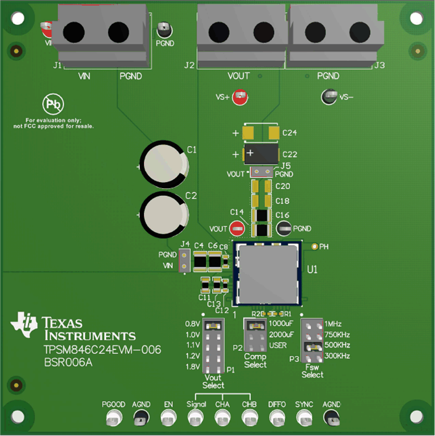
Figure 2-1 highlights the user interface items associated with the EVM. The polarized input power terminal block (TB1) is used for connection to the host input supply. TB2 allows two terminals for VOUT and TB3 allows two terminals for PGND for connection to the load. These terminal blocks can except up to 10-AWG wire.
 Figure 2-1 EVM User Interface
The VIN monitor (VIN and PGND) test points and VOUT monitor (VS+ and VS–) test points located near the input terminal block and the output terminal blocks are intended to be used as voltage monitoring points where voltmeters can be connected to measure the input and output voltages. Do not use these VIN and VOUT monitoring test points as the input supply or output load connection points. The PCB traces connecting to these test points are not designed to support high currents.
The VIN scope (J1) and VOUT scope (J2) test points can be used to monitor VIN and VOUT waveforms with an oscilloscope. These test points are intended for use with un-hooded scope probes outfitted with a low-inductance ground lead (ground spring) mounted to the scope probe barrel. The two sockets of each test point are on 0.1-inch centers. Insert the scope probe tip into the socket labeled VIN or VOUT, and insert the scope ground lead into the hole of the socket labeled PGND.
The test points located along the bottom of the EVM are made available to test the features of the device. Any external connections made to these test points should be referenced to one of the AGND test points. Refer to Section 3 for more information on the individual control test points.
The Vout Select jumper (P1) is used to set the output voltage. Select one of the five output voltages using a jumper. If a different voltage is required than the five selected using the jumper, leave the P1 jumper open and populate the correct resistor in position R2 on the EVM.
The Comp Select jumper (P2) sets the proper frequency compensation for the total amount of output capacitance present on the VOUT bus. The EVM is shipped with approximately 1000 µF of output capacitance loaded on the board. Locations are provided on the board to add additional output capacitance (C18–C21, C24, C25). The default Comp Select jumper is loaded in the 1000-µF position, which is the correct setting for output capacitance from 1000 µF to 1500 µF. The jumper position labeled 2000 µF selects compensation components for 1500 µF to 3000 µF of output capacitance. The jumper position labeled USER selects compensation components for 3000 µF to 5000 µF of output capacitance. See the TPSM846C24 4.5-V to 15-V Input, 0.5-V to 2.0-V Output, 35-A Power Module Data Sheet for more information on selecting compensation components.
The Fsw Select jumper (P3) is used to set the switching frequency. Select from 300 kHz, 500 kHz, 750 kHz, and 1 MHz. The default jumper loading is the 500-kHz position.