SNVU588A December   2017  – January 2022 TPS40345


  1.   Trademarks
  2. 1Description
    1. 1.1 Applications
    2. 1.2 Features
  3. 2TPS40345EVM-353 Electrical Performance Specifications
  4. 3TPS40345EVM-353 Schematic
  5. 4Connector and Test Point Descriptions
    1. 4.1 Enable Jumper (JP2)
    2. 4.2 Frequency Spread Spectrum – FSS Jumper (JP1)
    3. 4.3 Test Point Descriptions
      1. 4.3.1 Input Voltage Monitoring (TP1 and TP2)
      2. 4.3.2 Output Voltage Monitoring (TP3 and TP4)
      3. 4.3.3 Loop Response Testing (TP5, TP6, TP7, TP8, and R3)
      4. 4.3.4 Error Amplifier Voltage Monitoring (TP9, TP10, and TP11)
      5. 4.3.5 Switching Waveform Monitoring (TP12, TP13, TP14, and TP15)
      6. 4.3.6 Power-Good Voltage Monitoring (TP16 and TP18)
      7. 4.3.7 Enable and Soft-Start Voltage Monitoring (TP17 and TP18)
  6. 5Test Setup
    1. 5.1 Equipment
      1. 5.1.1 Voltage Source
      2. 5.1.2 Meters
      3. 5.1.3 Load
      4. 5.1.4 Oscilloscope
      5. 5.1.5 Recommended Wire Gauge
      6. 5.1.6 Other
    2. 5.2 Equipment Setup
      1. 5.2.1 Procedure
      2. 5.2.2 Diagram
    3. 5.3 Start-Up/Shutdown Procedure
    4. 5.4 Output Ripple Voltage Measurement Procedure
    5. 5.5 Control Loop Gain and Phase Measurement Procedure
    6. 5.6 Equipment Shutdown
  7. 6TPS40345EVM-353 Test Data
    1. 6.1 Efficiency
    2. 6.2 Line and Load Regulation
    3. 6.3 Output Voltage Ripple
    4. 6.4 Switch Node
    5. 6.5 Control Loop Bode Diagram
    6. 6.6 Additional Waveforms
      1. 6.6.1 Output Ripple With Frequency Spread Spectrum (FSS) Enabled
  8. 7TPS40345EVM-353 Assembly Drawings and Layout
  9. 8TPS40345EVM-353 Bill of Materials
  10. 9Revision History

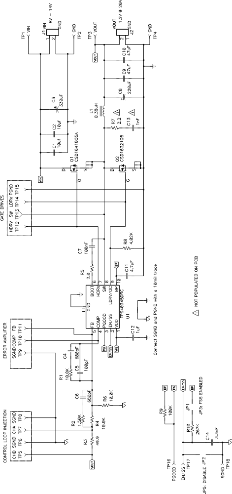
TPS40345EVM-353 Schematic

GUID-A88FEDC7-8A0B-4F3F-8F90-512AC799E76B-low.gif
For reference only, See Table 8-1 for specific values
Figure 3-1 TPS40345EVM-353 Schematic