SNVU658B March 2020 – May 2021 TPS54J060 , TPS54J061
- Trademarks
- 1Introduction
-
2Test Setup and Results
- 2.1 Input/Output Connections
- 2.2 Start Up Procedure
- 2.3 Efficiency
- 2.4 Load and Line Regulation
- 2.5 Load Transients
- 2.6 Loop Characteristics
- 2.7 Output Voltage Ripple
- 2.8 Input Voltage Ripple
- 2.9 Powering Up and Down with EN
- 2.10 Powering Up and Down With VIN
- 2.11 Start-Up Into Pre-Bias
- 2.12 Current Limit
- 3Schematic, List of Materials, and Layout
- Revision History
3.3 Layout
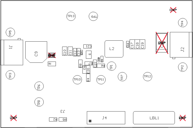
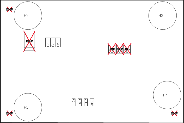
The board layout for the BSR067 PCB is shown in Figure 3-3 through Figure 3-10. The top-side layer of the EVM is laid out in a manner typical of a user application. The top, bottom, and internal layers are 2-oz. copper.
The top layer contains the main power traces for VIN, VOUT, and SW. Also on the top layer are connections for the remaining pins of the device and the majority of the signal traces. The top layer has a dedicated ground plane for quiet analog ground that is connected to the main power ground plane at a single point. Both internal planes contain a large ground plane. The bottom layer is another ground plane with two additional traces for the input and output voltage sense lines and various signals routed to test points and headers. There are also additional VIN and VOUT planes on the bottom layer. The top-side ground traces are connected to the bottom and internal ground planes with multiple via groupings placed around the board.
The input decoupling capacitors and bootstrap capacitor are all located as close to the IC as possible. Additionally, the voltage set point resistor divider components are kept close to the IC. Critical analog circuits that are noise sensitive are terminated to the quiet analog ground island on the top layer.
 Figure 3-3 Top-Side Assembly
 Figure 3-5 Top-Side Composite View
 Figure 3-7 Top-Side Layout
 Figure 3-9 Internal Layer-2 Layout
 Figure 3-4 Bottom-Side Assembly (Viewed From
Bottom)
 Figure 3-6 Bottom-Side Composite View (Viewed
From Bottom)
 Figure 3-8 Internal Layer-1 Layout
 Figure 3-10 Bottom-Side Layout (Viewed From
Top)