SNVU658B March 2020 – May 2021 TPS54J060 , TPS54J061
- Trademarks
- 1Introduction
-
2Test Setup and Results
- 2.1 Input/Output Connections
- 2.2 Start Up Procedure
- 2.3 Efficiency
- 2.4 Load and Line Regulation
- 2.5 Load Transients
- 2.6 Loop Characteristics
- 2.7 Output Voltage Ripple
- 2.8 Input Voltage Ripple
- 2.9 Powering Up and Down with EN
- 2.10 Powering Up and Down With VIN
- 2.11 Start-Up Into Pre-Bias
- 2.12 Current Limit
- 3Schematic, List of Materials, and Layout
- Revision History
2.8 Input Voltage Ripple
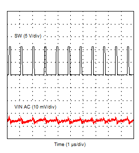
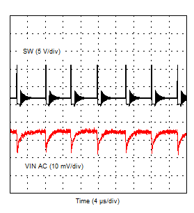
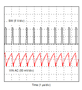
Figure 2-18, Figure 2-19, and Figure 2-20 show the TPS54J060EVM-067 and TPS54J061EVM-067 input voltage ripple for VIN = 12 V. The ripple voltage is measured directly across the ceramic input capacitor closest to the input terminal.
 Figure 2-18 Input Ripple – FCCM, 0.1-A Load
 Figure 2-20 Input Ripple – DCM, 0.1-A Load
 Figure 2-19 Input Ripple – FCCM, 6-A Load