SNVU658B March 2020 – May 2021 TPS54J060 , TPS54J061
- Trademarks
- 1Introduction
-
2Test Setup and Results
- 2.1 Input/Output Connections
- 2.2 Start Up Procedure
- 2.3 Efficiency
- 2.4 Load and Line Regulation
- 2.5 Load Transients
- 2.6 Loop Characteristics
- 2.7 Output Voltage Ripple
- 2.8 Input Voltage Ripple
- 2.9 Powering Up and Down with EN
- 2.10 Powering Up and Down With VIN
- 2.11 Start-Up Into Pre-Bias
- 2.12 Current Limit
- 3Schematic, List of Materials, and Layout
- Revision History
2.5 Load Transients
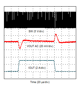
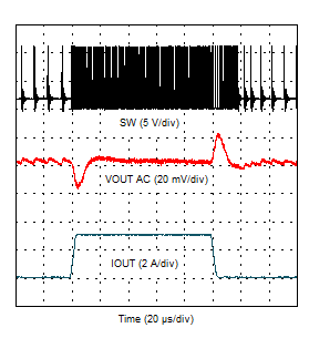
Figure 2-12 and Figure 2-13 shows how the TPS54J060EVM-067 and TPS54J061EVM-067 responds to load transients in FCCM and DCM respectively. The current step is from 0.1 to 3.1 A load. The current step slew rate is 1 A/µs. Total peak-to-peak voltage variation is as shown, including ripple and noise on the output.
 Figure 2-12 Load Transient Response – FCCM
 Figure 2-13 Load Transient Response – DCM