SNVU753A November   2019  – May 2021 TPS542A52


  1.   Trademarks
  2. 1Introduction
    1. 1.1 Before You Begin
  3. 2Description
    1. 2.1 Typical End-User Applications
    2. 2.2 EVM Features
    3. 2.3 TPS542A52EVM-059 PCB
  4. 3TPS542A52EVM-059 Bottom Circuit
    1. 3.1 Modifications
      1. 3.1.1 Output Voltage Setpoint
      2. 3.1.2 Enable and Undervoltage Lockout
      3. 3.1.3 External Clock Synchronization
      4. 3.1.4 Load Step with Function Generator
    2. 3.2 Bottom Circuit Schematic
    3. 3.3 Test Setup and Results
      1. 3.3.1  Input/Output Connections
      2. 3.3.2  Start Up Procedure
      3. 3.3.3  Electrical Performance Specifications and Results
      4. 3.3.4  Efficiency
      5. 3.3.5  Power Loss
      6. 3.3.6  Load Regulation
      7. 3.3.7  Transient Response
      8. 3.3.8  Loop Response
      9. 3.3.9  Output Voltage Ripple
      10. 3.3.10 Thermal Data
  5. 4TPS542A52EVM-059 Top Circuit (Small Layout Area Design)
    1. 4.1 Modifications
      1. 4.1.1 Output Voltage Setpoint
      2. 4.1.2 Enable and Undervoltage Lockout
      3. 4.1.3 External Clock Synchronization
      4. 4.1.4 Load Step with Function Generator
    2. 4.2 TPS542A52EVM-059 Top Circuit (Small Layout Area) Schematic
    3. 4.3 Test Setup and Results
      1. 4.3.1  Input/Output Connections
      2. 4.3.2  Start Up Procedure
      3. 4.3.3  Electrical Performance Specifications and Results
      4. 4.3.4  Efficiency
      5. 4.3.5  Power Loss
      6. 4.3.6  Load Regulation
      7. 4.3.7  Line Regulation
      8. 4.3.8  Transient Response
      9. 4.3.9  Loop Response
      10. 4.3.10 Output Voltage Ripple
      11. 4.3.11 Start Up
  6. 5TPS542A52EVM-059 PCB Layout
  7. 6List of Materials
  8. 7Revision History

TPS542A52EVM-059 PCB Layout

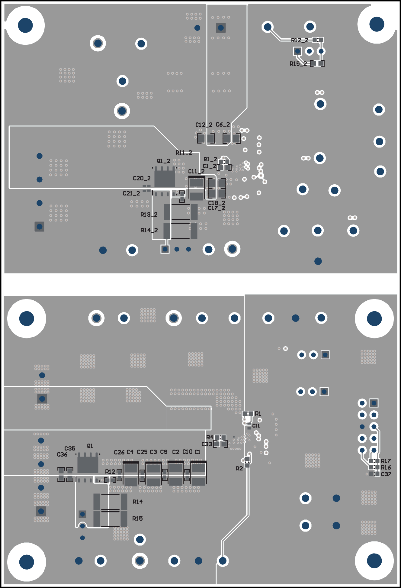
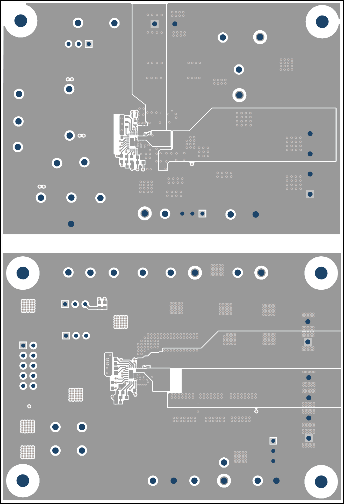
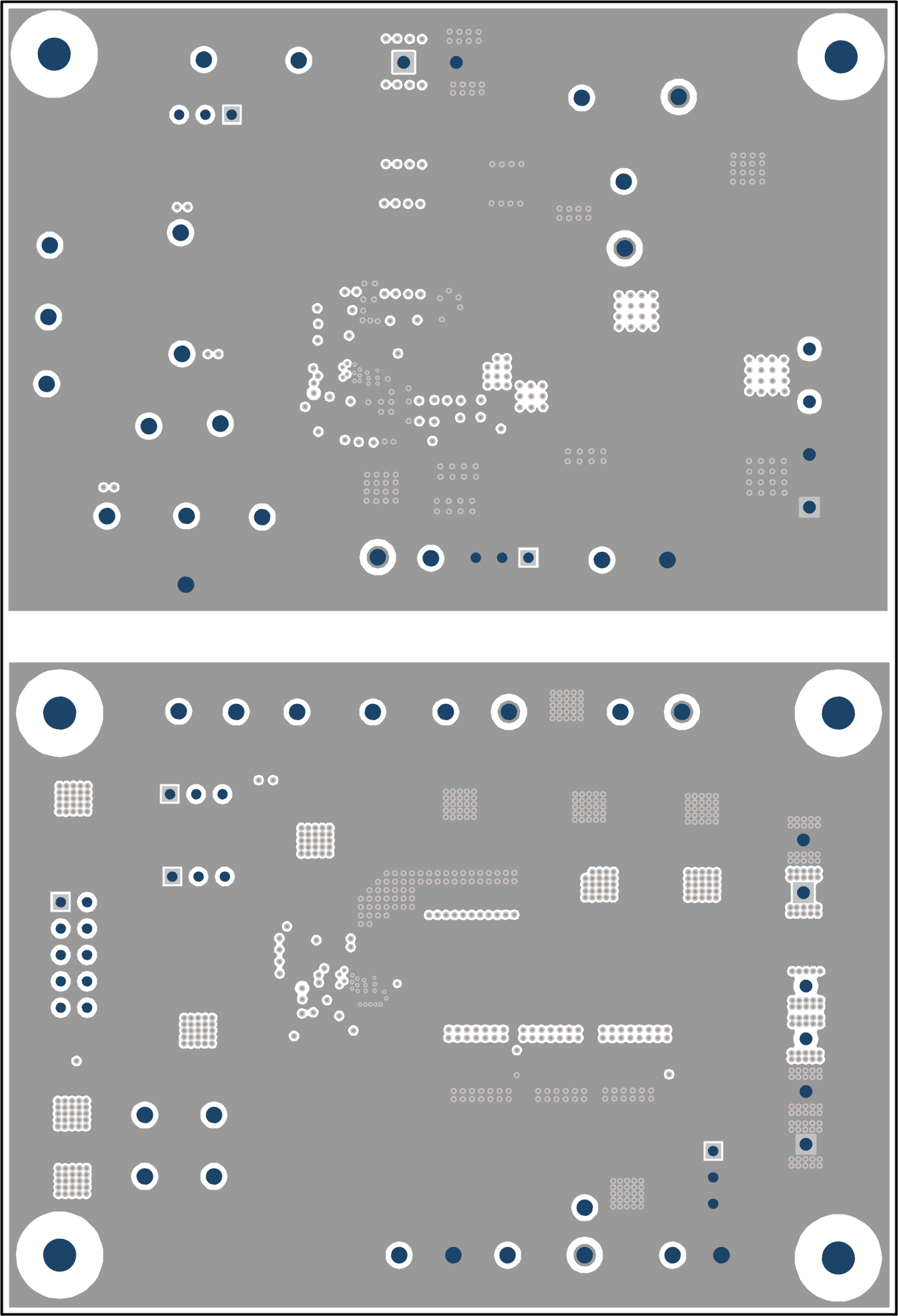
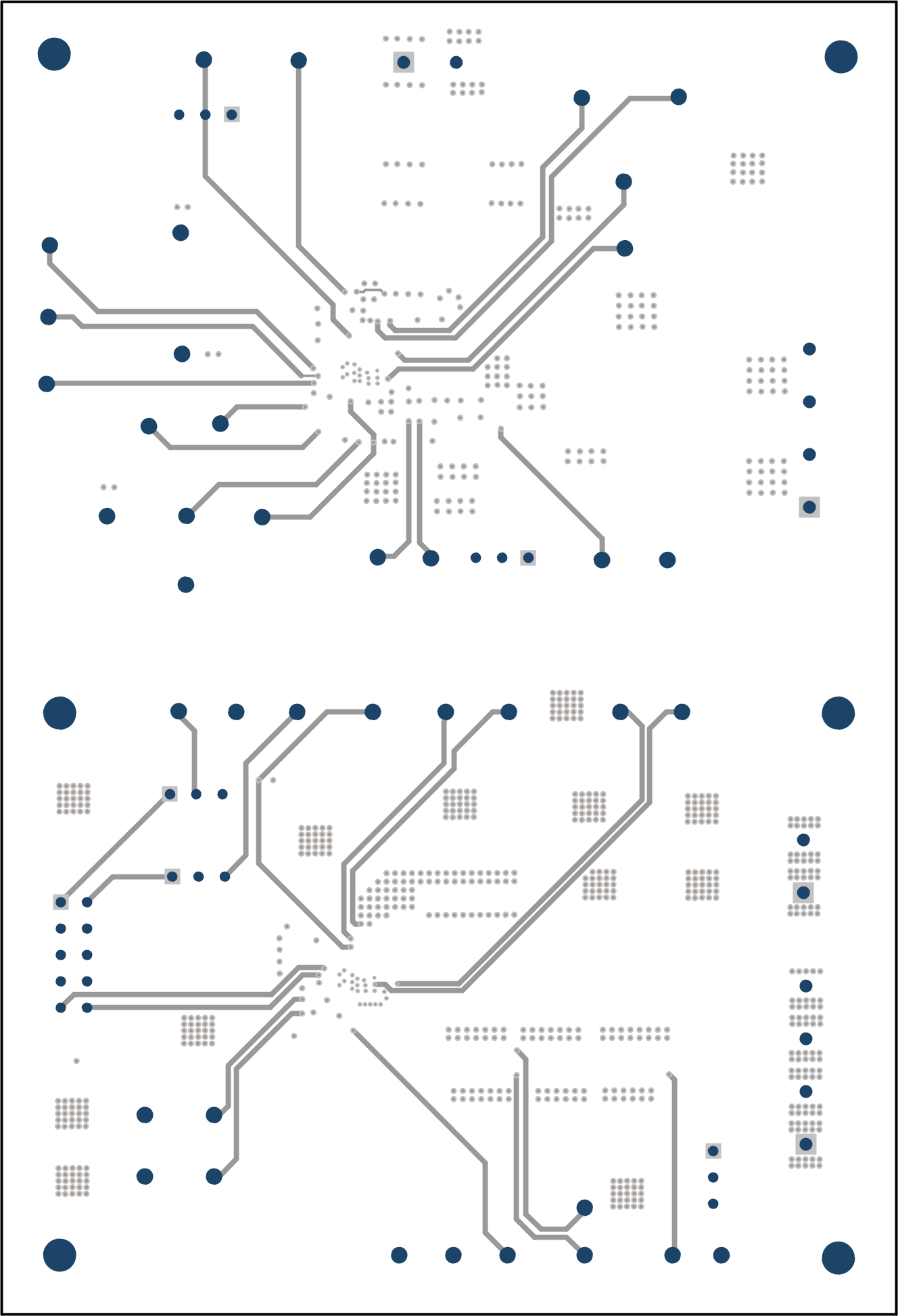
The PCB layout of the TPS542A52EVM-059 is shown in Figure 5-1 through Figure 5-8. The top, internal, and bottom layers are all 2 oz. copper.

GUID-20201020-CA0I-JZZM-S1FH-5SPMDPZFTGNG-low.svg Figure 5-1 Top-Side Composite View
GUID-20201020-CA0I-KLHL-XNLZ-WQG7SFVWR3HZ-low.gifFigure 5-2 Bottom-Side Composite View (Viewed From Bottom)
GUID-20201020-CA0I-MW2Q-RCCZ-4BBF0XGNSNRL-low.gifFigure 5-3 Top-Side Layout (Top-Down View)
GUID-20201020-CA0I-QGKC-JZQ4-RXG3XMRJL58Z-low.gifFigure 5-4 Internal Layer-1 Layout (Top-Down View)
GUID-20201020-CA0I-JXWD-9ZMN-MB9GSZTLHS1S-low.gifFigure 5-5 Internal Layer-2 Layout (Top-Down View)
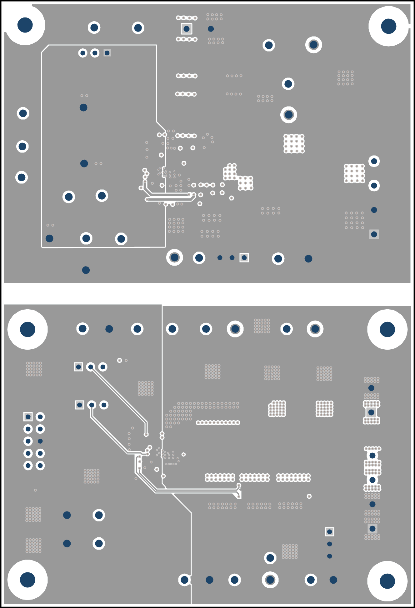
GUID-20201020-CA0I-SSPK-T8ZQ-WBXN52S7S3SV-low.gifFigure 5-6 Internal Layer-3 Layout (Top-Down View)
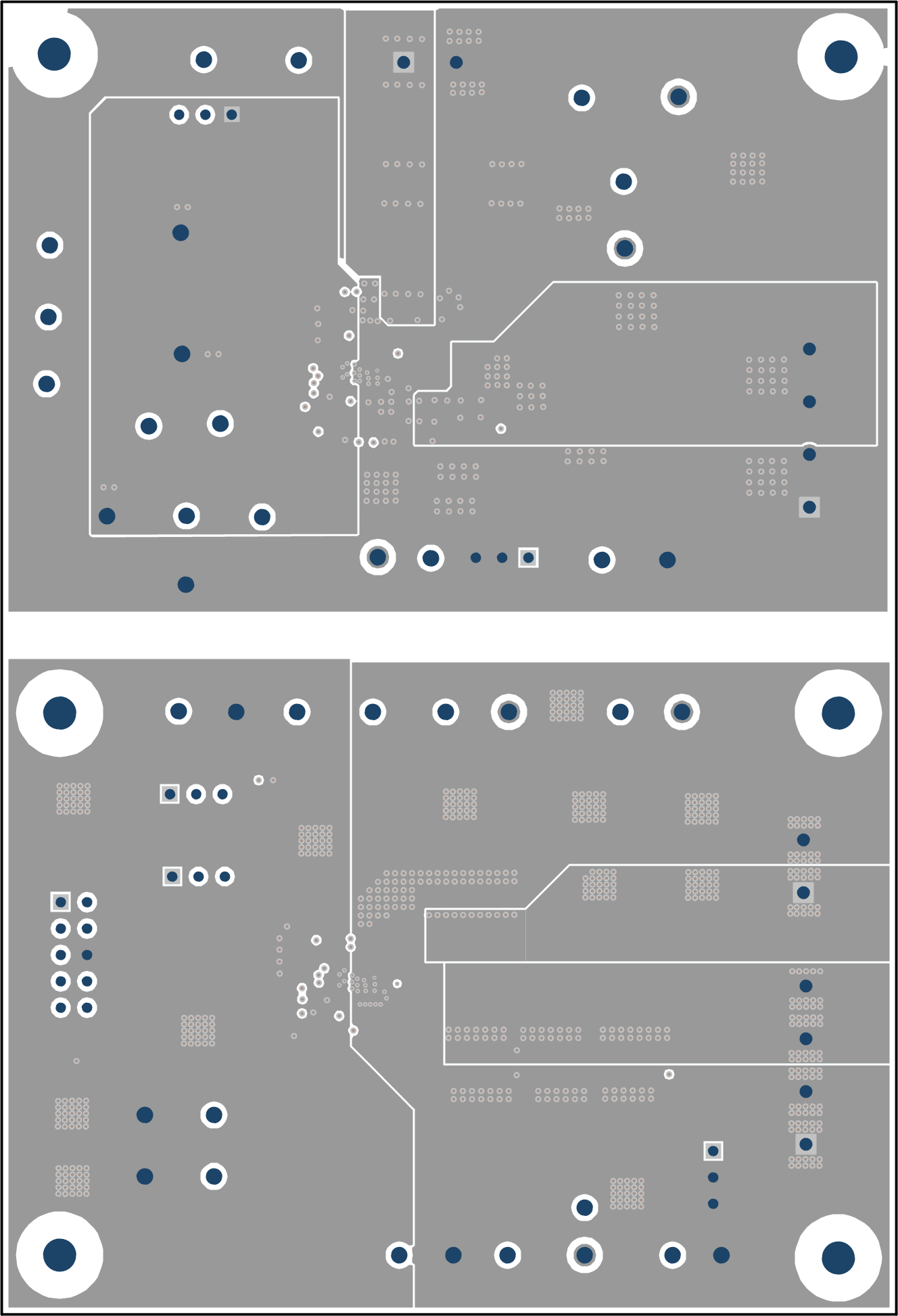
GUID-20201020-CA0I-TRWN-DRR7-QFV36C4DW3QV-low.gifFigure 5-7 Internal Layer-4 Layout (Top-Down View)
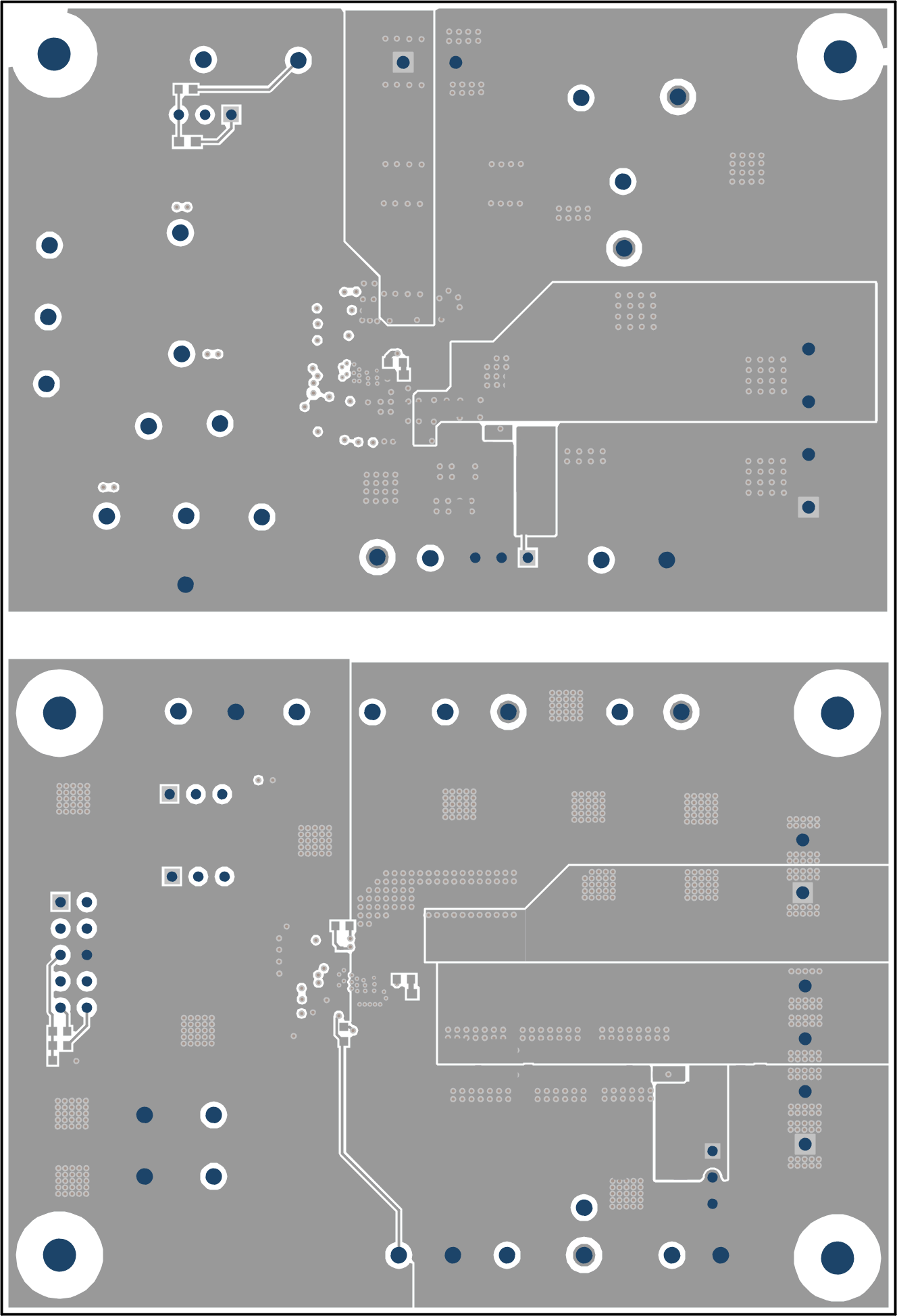
GUID-20201020-CA0I-D8ZH-HK1N-ZPKPFWLN8KHJ-low.gifFigure 5-8 Bottom-Side Layout (Top-Down View)