SNVU753A
November 2019 – May 2021
TPS542A52
Trademarks
1
Introduction
1.1
Before You Begin
2
Description
2.1
Typical End-User Applications
2.2
EVM Features
2.3
TPS542A52EVM-059 PCB
3
TPS542A52EVM-059 Bottom Circuit
3.1
Modifications
3.1.1
Output Voltage Setpoint
3.1.2
Enable and Undervoltage Lockout
3.1.3
External Clock Synchronization
3.1.4
Load Step with Function Generator
3.2
Bottom Circuit Schematic
3.3
Test Setup and Results
3.3.1
Input/Output Connections
3.3.2
Start Up Procedure
3.3.3
Electrical Performance Specifications and Results
3.3.4
Efficiency
3.3.5
Power Loss
3.3.6
Load Regulation
3.3.7
Transient Response
3.3.8
Loop Response
3.3.9
Output Voltage Ripple
3.3.10
Thermal Data
4
TPS542A52EVM-059 Top Circuit (Small Layout Area Design)
4.1
Modifications
4.1.1
Output Voltage Setpoint
4.1.2
Enable and Undervoltage Lockout
4.1.3
External Clock Synchronization
4.1.4
Load Step with Function Generator
4.2
TPS542A52EVM-059 Top Circuit (Small Layout Area) Schematic
4.3
Test Setup and Results
4.3.1
Input/Output Connections
4.3.2
Start Up Procedure
4.3.3
Electrical Performance Specifications and Results
4.3.4
Efficiency
4.3.5
Power Loss
4.3.6
Load Regulation
4.3.7
Line Regulation
4.3.8
Transient Response
4.3.9
Loop Response
4.3.10
Output Voltage Ripple
4.3.11
Start Up
5
TPS542A52EVM-059 PCB Layout
6
List of Materials
7
Revision History
3.3.6
Load Regulation
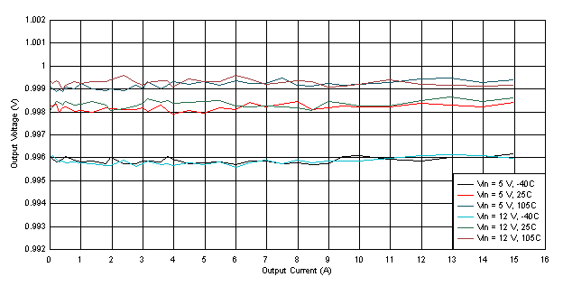
The EVM bottom circuit load regulation for ambient temperatures of -40°C to +105°C and input voltages of 5 V and 12 V is shown in
Figure 3-4
.
Figure 3-4
Load Regulation - FCCM, f
sw
= 1000 kHz, T
amb
= -40°C to +105°C