SNVU817 November 2021 LMR38020-Q1
4 PCB Layout
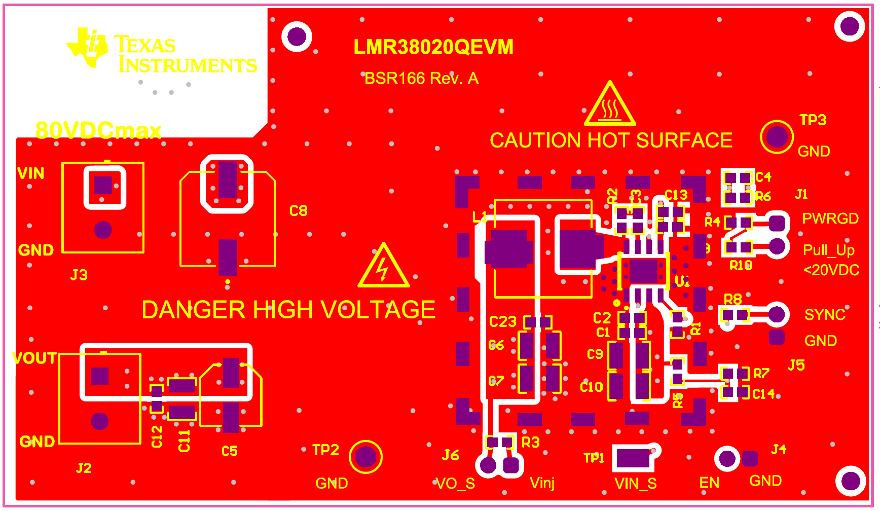
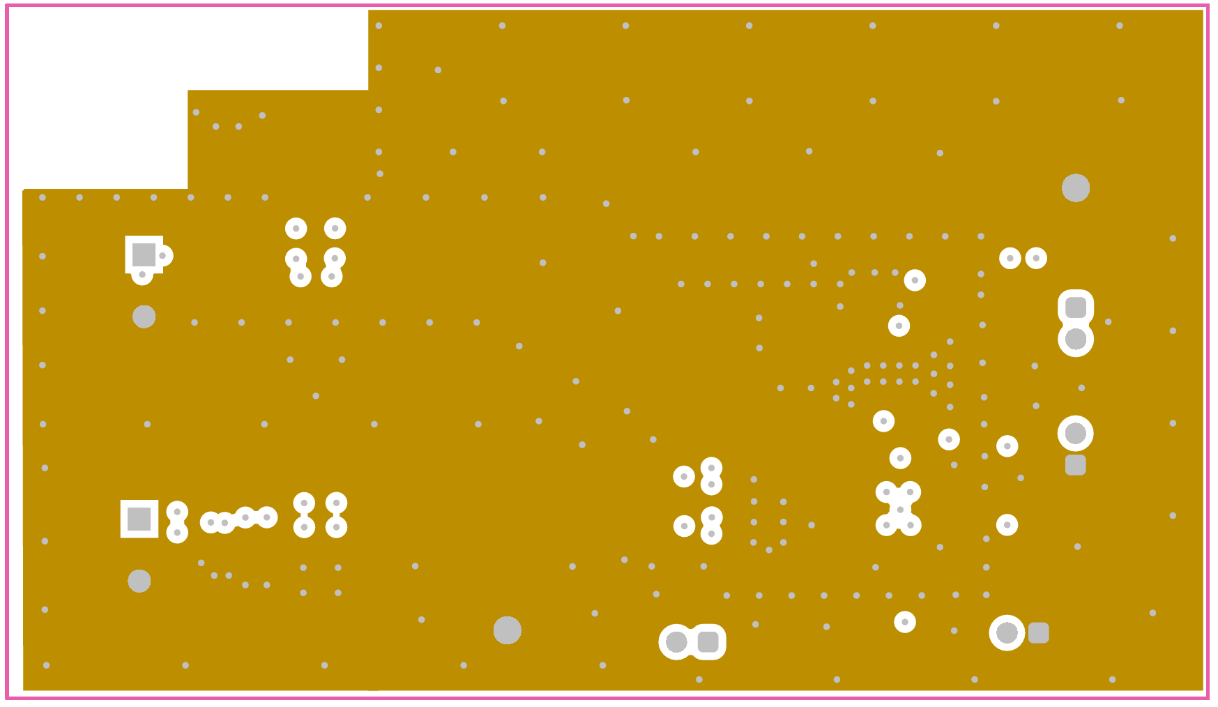
Figure 4-1 through Figure 4-4 show the board layout for the LMR38020QEVM. The EVM offers resistors, capacitors, and test points to configure the output voltage, precision enable, and switching frequency.
The 8-pin SO PowerPAD™ package offers an exposed thermal pad, which must be soldered to the copper landing on the PCB for optimal thermal performance. The PCB consists of a 4-layer design. There are 2-oz copper planes on the top and bottom and 1-oz copper mid-layer planes to dissipate heat with an array of thermal vias under the thermal pad to connect to all four layers.
Test points have been provided for ease of use to connect the power supply, required load, and to monitor critical signals.
 Figure 4-1 Top Layer and Silkscreen Layer
 Figure 4-2 Mid-Layer 1 Ground Plane
 Figure 4-3 Mid-Layer 2 Routing
 Figure 4-4 Bottom Layer Routing