SNVU883 December   2023


  1.   1
  2.   Description
  3.   Get Started
  4.   Features
  5.   Applications
  6.   6
  7. 1Evaluation Module Overview
    1. 1.1 Introduction
    2. 1.2 Kit Contents
    3. 1.3 Specification
    4. 1.4 Device Information
  8. 2Hardware
    1. 2.1 Additional Images
    2. 2.2 TPS389C0XEVM Hardware Setup
    3. 2.3 EVM Connectors
      1. 2.3.1 EVM Test Points
      2. 2.3.2 EVM Jumpers
    4. 2.4 EVM Setup and Operation
      1. 2.4.1 Example Operation of TPS389C0X-Q1
  9. 3Software
    1. 3.1 Setup and GUI Installations
      1. 3.1.1 TPS389C0XEVM Software Setup
    2. 3.2 Quick Start to TPS389C0XEVM GUI
  10. 4Hardware Design Files
    1. 4.1 TPS389C0XEVM Schematic
    2. 4.2 Layout and Component Placement
      1. 4.2.1 Layout
    3. 4.3 Bill of Materials
  11. 5Additional Information
    1.     Trademarks
  12. 6Related Documentation

TPS389C0XEVM Schematic

GUID-20231125-SS0I-PWJM-SLVT-3PSWGQKV1XTH-low.png Figure 4-1 TPS389C0XEVM Main Schematic
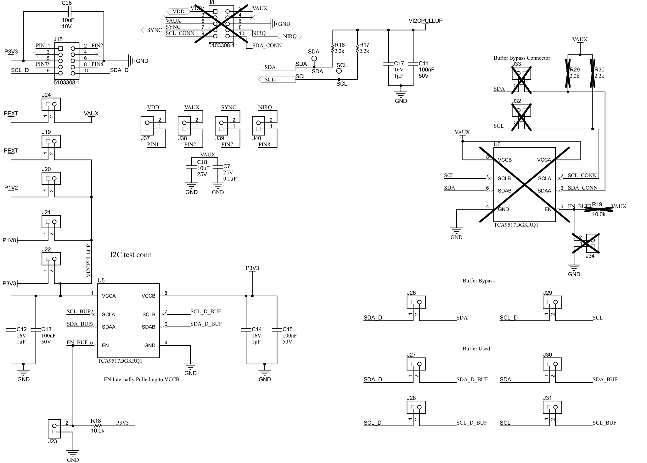
GUID-20231125-SS0I-ZQ0Q-5MZQ-8NFLH7WBLWCL-low.png Figure 4-2 TPS389C0XEVM I2C Schematic with Buffers