SNWA014 November 2023 LMH2110
2.2 Output Swing Derivation
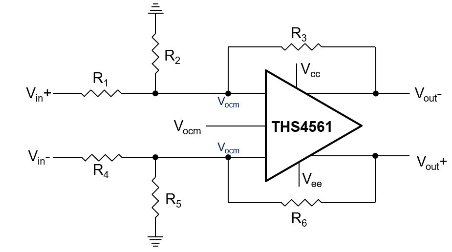
 Figure 2-2 THW4561 Output Swing Calculation Schematic
Our specification of interest, Vout,p-p (written as Vopp) is as below,
Both Vin+ and Vin- come from the outputs of the two power detectors, LMH2110. Vin+ represents the output from the forward power detector, similarly Vin- represents the same from the reflected power detector. Their difference is Vipp.
The THS4561 has an additional input, Vocm, that sets the common mode voltage of the device. By default, the device is set at the mid-point of the two supplies, Vcc and Vee for maximum differential output swing, however the device can be set by the user to control the output voltage swing.
In this example, the feedback resistor on both inputs are set to a fixed value, such as 2 kΩ. This enables easy calculation for the resistances in the divider network. The values of R1, R2, R4, and R5 can be derived for a given Vcc, Vee, Vipp and Vocm, and a desired Vopp.