SNWS022D January 2010 – June 2015 LMH2110
PRODUCTION DATA.
- 1 Features
- 2 Applications
- 3 Description
- 4 Revision History
- 5 Pin Configuration and Functions
- 6 Specifications
- 7 Detailed Description
-
8 Application and Implementation
- 8.1 Application Information
- 8.2 Typical Applications
- 9 Power Supply Recommendations
- 10Layout
- 11Device and Documentation Support
- 12Mechanical, Packaging, and Orderable Information
6 Specifications
6.1 Absolute Maximum Ratings
over operating free-air temperature range (unless otherwise noted)(1)(2)| MIN | MAX | UNIT | ||
|---|---|---|---|---|
| Supply voltage | VBAT – GND | 5.5 | V | |
| RF input | Input power | 12 | dBm | |
| DC voltage | 1 | V | ||
| Enable input voltage | GND – 0.4 < VEN and VEN< Min (VDD – 0.4 V, 3.6 V) | |||
| Junction temperature(3) | 150 | °C | ||
| Maximum lead temperature (Soldering,10 sec) | 260 | °C | ||
| Storage temperature, Tstg | −65 | 150 | °C | |
(1) Stresses beyond those listed under Absolute Maximum Ratings may cause permanent damage to the device. These are stress ratings only, which do not imply functional operation of the device at these or any other conditions beyond those indicated under Recommended Operating Conditions. Exposure to absolute-maximum-rated conditions for extended periods may affect device reliability.
(2) If Military/Aerospace specified devices are required, contact the Texas Instruments Sales Office/ Distributors for availability and specifications.
(3) The maximum power dissipation is a function of TJ(MAX), RθJA. The maximum allowable power dissipation at any ambient temperature is PD = (TJ(MAX) – TA)/RθJA. All numbers apply for packages soldered directly into a PC board.
6.2 ESD Ratings
| VALUE | UNIT | |||
|---|---|---|---|---|
| V(ESD) | Electrostatic discharge | Human-body model (HBM), per ANSI/ESDA/JEDEC JS-001(1) | ±2000 | V |
| Charged-device model (CDM), per JEDEC specification JESD22-C101(2) | ±1000 | |||
| Machine Model | ±200 | |||
(1) JEDEC document JEP155 states that 500-V HBM allows safe manufacturing with a standard ESD control process.
(2) JEDEC document JEP157 states that 250-V CDM allows safe manufacturing with a standard ESD control process.
6.3 Recommended Operating Conditions
over operating free-air temperature range (unless otherwise noted)(1)| MIN | MAX | UNIT | ||
|---|---|---|---|---|
| Supply voltage | 2.7 | 5 | V | |
| Operating temperature | −40 | 85 | °C | |
| RF frequency | 50 | 8000 | MHz | |
| RF input power | −40 | 5 | dBm | |
(1) Stresses beyond those listed under Absolute Maximum Ratings may cause permanent damage to the device. These are stress ratings only, which do not imply functional operation of the device at these or any other conditions beyond those indicated under Recommended Operating Conditions. Exposure to absolute-maximum-rated conditions for extended periods may affect device reliability.
6.4 Thermal Information
| THERMAL METRIC(1) | LMH2110 | UNIT | |
|---|---|---|---|
| YFQ (DSBGA) | |||
| 6 PINS | |||
| RθJA | Junction-to-ambient thermal resistance | 133.7 | °C/W |
| RθJC(top) | Junction-to-case (top) thermal resistance | 1.7 | °C/W |
| RθJB | Junction-to-board thermal resistance | 22.6 | °C/W |
| ψJT | Junction-to-top characterization parameter | 5.7 | °C/W |
| ψJB | Junction-to-board characterization parameter | 22.2 | °C/W |
(1) For more information about traditional and new thermal metrics, see the Semiconductor and IC Package Thermal Metrics application report, SPRA953.
6.5 2.7-V and 4.5-V DC and AC Electrical Characteristics
Unless otherwise specified: all limits are ensured to TA = 25°C, VBAT = 2.7 V and 4.5 V (worst of the 2 is specified),RFIN = 1900 MHz CW (Continuous Wave, unmodulated).(1)
| PARAMETER | TEST CONDITIONS | MIN(2) | TYP(3) | MAX(2) | UNIT | ||
|---|---|---|---|---|---|---|---|
| SUPPLY INTERFACE | |||||||
| IBAT | Supply current | Active mode: EN = HIGH, no signal present at RFIN | 3.7 | 4.8 | 5.5 | mA | |
| Active mode: EN = HIGH, no signal present at RFIN
Limits apply at temperature extremes. |
2.9 | 5.9 | |||||
| Shutdown: EN = LOW, no signal present at RFIN. | VBAT = 2.7 V | 3.7 | 4.7 | μA | |||
| VBAT = 4.5 V | 4.6 | 5.7 | |||||
| Shutdown: EN = LOW, no signal present at RFIN. Limits apply at temperature extremes. |
VBAT = 2.7 V | 5 | μA | ||||
| VBAT = 4.5 V | 6.1 | ||||||
| EN = Low, RFIN = 0 dBm, 1900 MHz | VBAT = 2.7V | 3.5 | 4.7 | μA | |||
| VBAT = 4.5 V | 4.6 | 5.7 | |||||
| EN = Low, RFIN = 0 dBm, 1900 MHz Limits apply at temperature extremes. |
VBAT = 2.7 V | 5 | μA | ||||
| VBAT = 4.5 V | 6.1 | ||||||
| PSRR | Power Supply Rejection Ratio(4) | RFIN = −10 dBm, 1900 MHz, 2.7V < VBAT < 5 V | 56 | dB | |||
| RFIN = −10 dBm, 1900 MHz, 2.7V < VBAT < 5 V Limits apply at temperature extremes. |
45 | ||||||
| LOGIC ENABLE INTERFACE | |||||||
| VLOW | EN logic low input level (Shutdown mode) | Limits apply at temperature extremes. | 0.6 | V | |||
| VHIGH | EN logic high input level | Limits apply at temperature extremes. | 1.1 | V | |||
| IEN | Current into EN pin | Limits apply at temperature extremes. | 50 | nA | |||
| INPUT/OUTPUT INTERFACE | |||||||
| RIN | Input resistance | 44 | 50 | 56 | Ω | ||
| VOUT | Minimum output voltage (pedestal) | No input signal | 1.5 | mV | |||
| No input signal, limits apply at temperature extremes | 0 | 8 | |||||
| ROUT | Output impedance | EN = High, RFIN = –10 dBm, 1900 MHz, ILOAD = 1 mA, DC measurement | 0.2 | 2 | Ω | ||
| EN = High, RFIN = –10 dBm, 1900 MHz, ILOAD = 1 mA, DC measurement, limits apply at temperature extremes. |
3 | ||||||
| IOUT | Output short circuit current | Sinking, RFIN = –10 dBm, OUT connected to 2.5 V | 37 | 42 | mA | ||
| Sinking, RFIN = –10 dBm, OUT connected to 2.5 V Limits apply at temperature extremes. |
32 | ||||||
| Sourcing, RFIN = –10 dBm, OUT connected to GND | 40 | 46 | |||||
| Sourcing, RFIN = –10 dBm, OUT connected to GND Limits apply at temperature extremes. |
34 | ||||||
| IOUT,SD | Output leakage current in shutdown mode | EN = Low, OUT connected to 2 V Limits apply at temperature extremes. |
50 | nA | |||
| en | Output referred noise(4) | RFIN = −10 dBm, 1900 MHz, output spectrum at 10 kHz | 3 | µV√Hz | |||
| VN | Integrated output referred noise(4) | Integrated over frequency band 1 kHz – 6.5 kHz, RFIN = –10 dBm, 1900 MHz |
210 | µVRMS | |||
| RF DETECTOR TRANSFER
RFIN = 50 MHz (fit range –20 dBm to –10 dBm)(5) |
|||||||
| PMIN | Minimum power level, bottom end of dynamic range | Log conformance error within ±1 dB | –39 | dBm | |||
| PMAX | Maximum power level, top end of dynamic range | Log conformance error within ±1 dB | 7 | dBm | |||
| VMIN | Minimum output voltage | At PMIN | 3 | mV | |||
| VMAX | Maximum output voltage | At PMAX | 1.96 | V | |||
| KSLOPE | Logarithmic slope | 42.2 | 44.3 | 46.4 | mV/dB | ||
| PINT | Logarithmic Intercept | –38.6 | –38.3 | –38.0 | dBm | ||
| DR | Dynamic Range for specified accuracy | ±1-dB Log conformance error (ELC) | 46 | dB | |||
| ±1-dB Log conformance error (ELC) Limits apply at temperature extremes. |
45 | ||||||
| ±3-dB Log Conformance Error (ELC) | 51 | ||||||
| ±3-dB Log conformance error (ELC) Limits apply at temperature extremes. |
50 | ||||||
| ±0.5-dB input referred variation over temperature (EVOT), from PMIN
Limits apply at temperature extremes. |
42 | ||||||
| RF DETECTOR TRANSFER
RFIN = 900 MHz (fit range –20 dBm to –10 dBm)(5) |
|||||||
| PMIN | Minimum power level, bottom end of dynamic range | Log conformance error within ±1 dB | –38 | dBm | |||
| PMAX | Maximum power level, top end of dynamic range | Log conformance error within ±1 dB | 0 | dBm | |||
| VMIN | Minimum output voltage | At PMIN | 3 | mV | |||
| VMAX | Maximum output voltage | At PMAX | 1.58 | V | |||
| KSLOPE | Logarithmic slope | 41.8 | 43.9 | 46 | mV/dB | ||
| PINT | Logarithmic intercept | –37.4 | –37 | –36.7 | dBm | ||
| DR | Dynamic range for specified accuracy | ±1-dB Log conformance error (ELC) | 38 | dB | |||
| ±1-dB Log conformance error (ELC) Limits apply at temperature extremes. |
37 | ||||||
| ±3-dB Log conformance error (ELC) | 45 | ||||||
| ±3-dB Log conformance error (ELC) Limits apply at temperature extremes. |
44 | ||||||
| ±0.5-dB Input referred variation over temperature (EVOT), from PMIN
Limits apply at temperature extremes. |
44 | ||||||
| ±0.3-dB Error for a 1dB Step (E1dB STEP) | 41 | ||||||
| ±0.3-dB Error for a 1dB Step (E1dB STEP) Limits apply at temperature extremes. |
38 | ||||||
| ±1-dB Error for a 10dB Step (E10dB 30 STEP) Limits apply at temperature extremes. |
32 | ||||||
| EMOD | Input-referred variation due to modulation | W-CDMA Release 6/7/8, –38 dBm < RFIN < –5 dBm |
0.08 | dB | |||
| LTE, –38 dBm < RFIN < –5 dBm | 0.19 | ||||||
| RF DETECTOR TRANSFER
RFIN = 1900 MHz (fit range –20 dBm to –10 dBm)(5) |
|||||||
| PMIN | Minimum power level, bottom end of dynamic range | Log conformance error within ±1 dB | –36 | dBm | |||
| PMAX | Maximum power level, top end of dynamic range | Log conformance error within ±1 dB | 0 | dBm | |||
| VMIN | Minimum output voltage | At PMIN | 3 | mV | |||
| VMAX | maximum output voltage | At PMAX | 1.5 | V | |||
| KSLOPE | Logarithmic slope | 41.8 | 43.9 | 46.1 | mV/dB | ||
| PINT | Logarithmic Intercept | –35.5 | –35.1 | –34.7 | dBm | ||
| DR | Dynamic range for specified accuracy | ±1-dB Log conformance error (ELC) Limits apply at temperature extremes. |
36 | dB | |||
| ±3-dB Log conformance Error (ELC) | 45 | ||||||
| ±3-dB Log conformance error (ELC) Limits apply at temperature extremes. |
43 | ||||||
| ±0.5-dB Input referred variation over temperature (EVOT), from PMIN
Limits apply at temperature extremes. |
41 | ||||||
| ±0.3-dB error for a 1-dB Step (E1dB STEP) | 40 | ||||||
| ±0.3-dB error for a 1-dB Step (E1dB STEP) Limits apply at temperature extremes. |
38 | ||||||
| ±1-dB error for a 10-dB Step (E10-dB 30 STEP) Limits apply at temperature extremes. |
30 | ||||||
| EMOD | Input-referred variation due to modulation | W-CDMA Release 6/7/8, –38 dBm < RFIN < –5 dBm |
0.09 | dB | |||
| LTE, –38 dBm < RFIN < –5 dBm | 0.18 | ||||||
| RFIN = 3500 MHz, fit range –15 dBm to –5 dBm(5) | |||||||
| PMIN | Minimum power level, bottom end of dynamic range | Log conformance error within ±1 dB | –31 | dBm | |||
| PMAX | Maximum power level, top end of dynamic range | Log conformance error within ±1 dB | 6 | dBm | |||
| VMIN | Minimum output voltage | At PMIN | 2 | mV | |||
| VMAX | Maximum output voltage | At PMAX | 1.52 | V | |||
| KSLOPE | Logarithmic slope | 41.8 | 44 | 46.1 | mV/dB | ||
| PINT | Logarithmic Intercept | –30.5 | –29.7 | –28.8 | dBm | ||
| DR | Dynamic range for specified accuracy | ±1-dB Log conformance error (ELC) | 37 | dB | |||
| ±1-dB Log conformance error (ELC) Limits apply at temperature extremes. |
36 | ||||||
| ±3-dB Log conformance error (ELC) | 44 | ||||||
| ±3-dB Log conformance error (ELC) Limits apply at temperature extremes. |
42 | ||||||
| ±0.5-dB Input referred variation over temperature (EVOT), from PMIN
Limits apply at temperature extremes. |
39 | ||||||
| RFIN = 5800 MHz, fit range –20 dBm to 3 dBm(5) | |||||||
| PMIN | Minimum power level, bottom end of dynamic range | Log conformance error within ±1 dB | –22 | dBm | |||
| PMAX | Maximum power level, top end of dynamic range | Log conformance error within ±1 dB | 10 | dBm | |||
| VMIN | Minimum output voltage | At PMIN | 3 | mV | |||
| VMAX | Maximum output voltage | At PMAX | 1.34 | V | |||
| KSLOPE | Logarithmic slope | 42.5 | 44.8 | 47.1 | mV/dB | ||
| PINT | Logarithmic Intercept | –22 | –21 | –19.9 | dBm | ||
| DR | Dynamic range for specified accuracy | ±1-dB Log conformance error (ELC) | 32 | dB | |||
| ±1-dB Log conformance error (ELC) Limits apply at temperature extremes. |
31 | ||||||
| ±3-dB Log conformance error (ELC) | 39 | ||||||
| ±3-dB Log conformance error (ELC) Limits apply at temperature extremes. |
37 | ||||||
| ±0.5-dB Input referred variation over temperature (EVOT), from PMIN
Limits apply at temperature extremes. |
33 | ||||||
(1) 2.7-V and 4.5-V DC and AC Electrical Characteristics values apply only for factory testing conditions at the temperature indicated. Factory testing conditions result in very limited self-heating of the device such that TJ = TA. Parametric performance is not ensured in the 2.7-V and 4.5-V DC and AC Electrical Characteristics under conditions of internal self-heating where TJ > TA.
(2) All limits are specified by test or statistical analysis.
(3) Typical values represent the most likely parametric norm as determined at the time of characterization. Actual typical values may vary over time and depend on the application and configuration. The typical values are not tested and are not specified on shipped production material.
(4) This parameter is specified by design and/or characterization and is not tested in production.
(5) All limits are specified by design and measurements which are performed on a limited number of samples. Limits represent the mean ±3–sigma values. The typical value represents the statistical mean value.
6.6 Timing Requirements
| MIN | NOM | MAX | UNIT | ||
|---|---|---|---|---|---|
| tON | Turnon time from shutdown RFIN = –10 dBm, 1900 MHz, EN LOW-HIGH transition to OUT at 90% |
15 | 19 | µs | |
| tR | Rise time(1)
Signal at RFIN from –20 dBm to 0 dBm, 10% to 90%, 1900 MHz |
2.2 | µs | ||
| tF | Fall time (1)
Signal at RFIN from 0 dBm to –20 dBm, 90% to 10%, 1900 MHz |
31 | µs | ||
(1) This parameter is specified by design and/or characterization and is not tested in production.
6.7 Typical Characteristics
Unless otherwise specified: TA = 25°C, VBAT = 2.7 V, RFIN = 1900 MHz CW (Continuous Wave, unmodulated). Specified errors are input referred.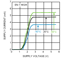 Figure 1. Supply Current vs. Supply Voltage (Active)
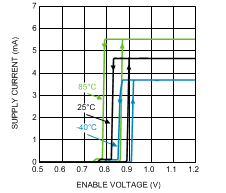 Figure 3. Supply Current vs. Enable Voltage (EN)
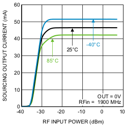 Figure 5. Sourcing Output Current vs. RF Input Power
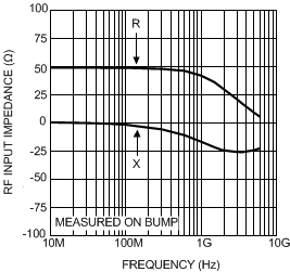 Figure 7. RF Input Impedance vs. Frequency,
Resistance (R) and Reactance (X)
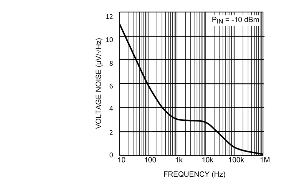 Figure 9. Output Voltage Noise vs. Frequency
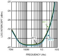 Figure 11. Log Intercept vs. Frequency
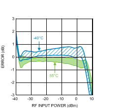 Figure 13. Log Conformance Error (50 Units) vs.
RF Input Power at 50 MHz
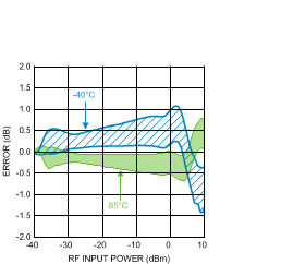 Figure 15. Temperature Variation (50 Units) vs.
RF Input Power at 50 MHz
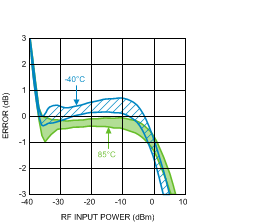 Figure 17. Log Conformance Error (50 Units) vs.
RF Input Power at 900 MHz
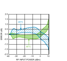 Figure 19. Temperature Variation (50 Units) vs.
RF Input Power at 900 MHz
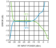 Figure 21. 10 dB Power Step Error vs.
RF Input Power at 900 MHz
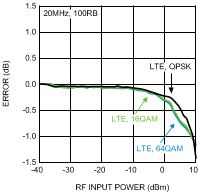 Figure 23. LTE Variation vs.
RF Input Power at 900 MHz
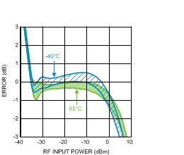 Figure 25. Log Conformance Error (50 Units) vs.
RF Input Power at 1900 MHz
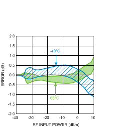 Figure 27. Temperature Variation (50 Units) vs.
RF Input Power at 1900 MHz
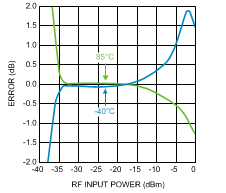 Figure 29. 10-dB Power Step Error vs.
RF Input Power at 1900 MHz
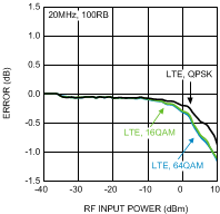 Figure 31. LTE Input referred Variation vs.
RF Input Power at 1900 MHz
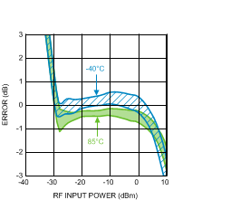 Figure 33. Log Conformance Error (50 Units) vs.
RF Input Power at 3500 MHz
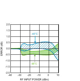 Figure 35. Temperature Variation (50 Units) vs.
RF Input Power at 3500 MHz
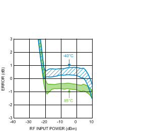 Figure 37. Log Conformance Error (50 Units) vs.
RF Input Power at 5800 MHz
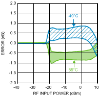 Figure 39. Temperature Variation (50 Units) vs.
RF Input Power at 5800 MHz
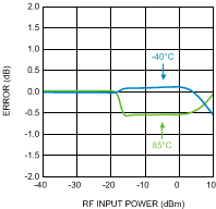 Figure 41. Temperature Variation vs.
RF Input Power at 8000 MHz
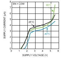 Figure 2. Supply Current vs. Supply Voltage (Shutdown)
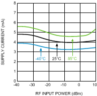 Figure 4. Supply Current vs. RF Input Power
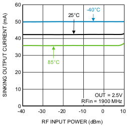 Figure 6. Sinking Output Current vs. RF Input Power
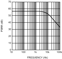 Figure 8. Power Supply Rejection Ratio vs. Frequency
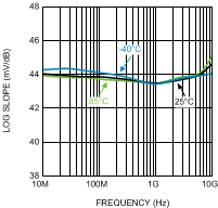 Figure 10. Log Slope vs. Frequency
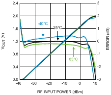 Figure 12. Output Voltage and Log Conformance Error vs.
RF Input Power at 50 MHz
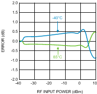 Figure 14. Temperature Variation vs.
RF Input Power at 50 MHz
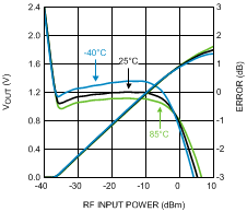 Figure 16. Output Voltage and Log Conformance Error vs.
RF Input Power at 900 MHz
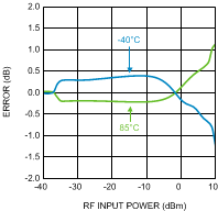 Figure 18. Temperature Variation vs.
RF Input Power at 900 MHz
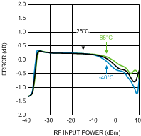 Figure 20. 1-dB Power Step Error vs.
RF Input Power at 900 MHz
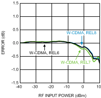 Figure 22. W-CDMA Variation vs.
RF Input Power at 900 MHz
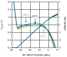 Figure 24. Output Voltage and Log Conformance Error vs.
RF Input Power at 1900 MHz
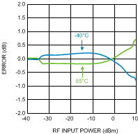 Figure 26. Temperature Variation vs.
RF Input Power at 1900 MHz
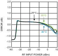 Figure 28. 1-dB Power Step Error vs.
RF Input Power at 1900 MHz
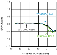 Figure 30. W-CDMA Variation vs.
RF Input Power at 1900 MHz
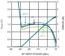 Figure 32. Output Voltage and Log Conformance Error vs.
RF Input Power at 3500 MHz
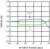 Figure 34. Temperature Variation vs.
RF Input Power at 3500 MHz
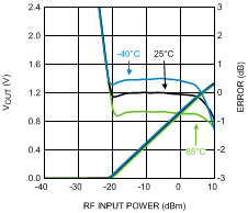 Figure 36. Output Voltage and Log Conformance Error vs.
RF Input Power at 5800 MHz
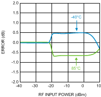 Figure 38. Temperature Variation vs.
RF Input Power at 5800 MHz
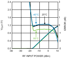 Figure 40. Output Voltage and Log Conformance Error vs.
RF Input Power at 8000 MHz