SPAU023 June   2024


  1.   1
  2.   Description
  3.   Features
  4.   4
  5. 1Evaluation Module Overview
    1. 1.1 Introduction
    2. 1.2 Kit Contents
  6. 2Hardware
    1. 2.1 System Description
      1. 2.1.1 Key Features
        1. 2.1.1.1 Power Supply
        2. 2.1.1.2 Memory
        3. 2.1.1.3 JTAG Emulator
        4. 2.1.1.4 Supported Interfaces and Peripherals
        5. 2.1.1.5 Expansion Connectors/Headers to Support Application-specific Add‐On Boards
        6. 2.1.1.6 ADC
      2. 2.1.2 Important Usage Notes:
        1. 2.1.2.1 Electrostatic Discharge (ESD) Compliance
        2. 2.1.2.2 IO Cable Length
      3. 2.1.3 Functional Block Diagram
      4. 2.1.4 Power ON/OFF Procedures
        1. 2.1.4.1 Power-On Procedure
        2. 2.1.4.2 Power-Off Procedure
        3. 2.1.4.3 Power Test Points
      5. 2.1.5 Peripheral and Major Component Description
        1. 2.1.5.1 Clocking
        2. 2.1.5.2 EtherCAT Interface
          1. 2.1.5.2.1 DP83826 PHY Strapping Configuration
        3. 2.1.5.3 Power
          1. 2.1.5.3.1 Power Requirement
          2. 2.1.5.3.2 Power Input
        4. 2.1.5.4 Emulator Connector (TSW-106-16-G-D) and DAC Connector (TSW-102-16-G-D)
          1. 2.1.5.4.1 TSW-106-16-G-D
          2. 2.1.5.4.2 TSW-102-16-G-D
        5. 2.1.5.5 FSI Header
        6. 2.1.5.6 High Density Connector
          1. 2.1.5.6.1 180-pin HSEC Edge Connector
        7. 2.1.5.7 Use Case for HSEC Adapter Board
          1. 2.1.5.7.1 Case 1: Isolated XDS110 on HSEC Adapter, SOM ,Baseboard
          2. 2.1.5.7.2 Case 2: HSEC Adapter, Isolated XDS110 on SOM, Baseboard
  7. 3Hardware Design Files
  8. 4Additional Information
    1. 4.1 Trademarks

Clocking

The Clock architecture of the HSEC Adapter board is shown below.
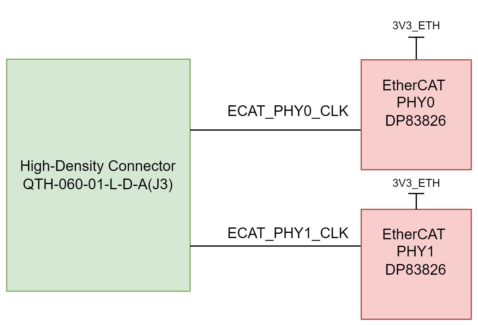
HSEC180ADAPEVM Clock Architecture Figure 2-5 Clock Architecture

A clock generator of part number LMK1C1103PWR is used in SOM to drive the 25MHz clock to two EtherCATPHYs, and F28P65x MCU Clock. LMK1C1103PWR is a 1:3 LVCMOS clock buffer, which takes the 25MHz crystal/LVCMOS reference input and provides four 25MHz LVCMOS clock outputs. The clock signal for EtherCAT PHYs is routed from SOM to High-density connector.