SPAU023
June 2024
1
Description
Features
4
1
Evaluation Module Overview
1.1
Introduction
1.2
Kit Contents
2
Hardware
2.1
System Description
2.1.1
Key Features
2.1.1.1
Power Supply
2.1.1.2
Memory
2.1.1.3
JTAG Emulator
2.1.1.4
Supported Interfaces and Peripherals
2.1.1.5
Expansion Connectors/Headers to Support Application-specific Add‐On Boards
2.1.1.6
ADC
2.1.2
Important Usage Notes:
2.1.2.1
Electrostatic Discharge (ESD) Compliance
2.1.2.2
IO Cable Length
2.1.3
Functional Block Diagram
2.1.4
Power ON/OFF Procedures
2.1.4.1
Power-On Procedure
2.1.4.2
Power-Off Procedure
2.1.4.3
Power Test Points
2.1.5
Peripheral and Major Component Description
2.1.5.1
Clocking
2.1.5.2
EtherCAT Interface
2.1.5.2.1
DP83826 PHY Strapping Configuration
2.1.5.3
Power
2.1.5.3.1
Power Requirement
2.1.5.3.2
Power Input
2.1.5.4
Emulator Connector (TSW-106-16-G-D) and DAC Connector (TSW-102-16-G-D)
2.1.5.4.1
TSW-106-16-G-D
2.1.5.4.2
TSW-102-16-G-D
2.1.5.5
FSI Header
2.1.5.6
High Density Connector
2.1.5.6.1
180-pin HSEC Edge Connector
2.1.5.7
Use Case for HSEC Adapter Board
2.1.5.7.1
Case 1: Isolated XDS110 on HSEC Adapter, SOM ,Baseboard
2.1.5.7.2
Case 2: HSEC Adapter, Isolated XDS110 on SOM, Baseboard
3
Hardware Design Files
4
Additional Information
4.1
Trademarks
2.1.3
Functional Block Diagram
The functional block diagram of the HSEC adapter Board is shown below.
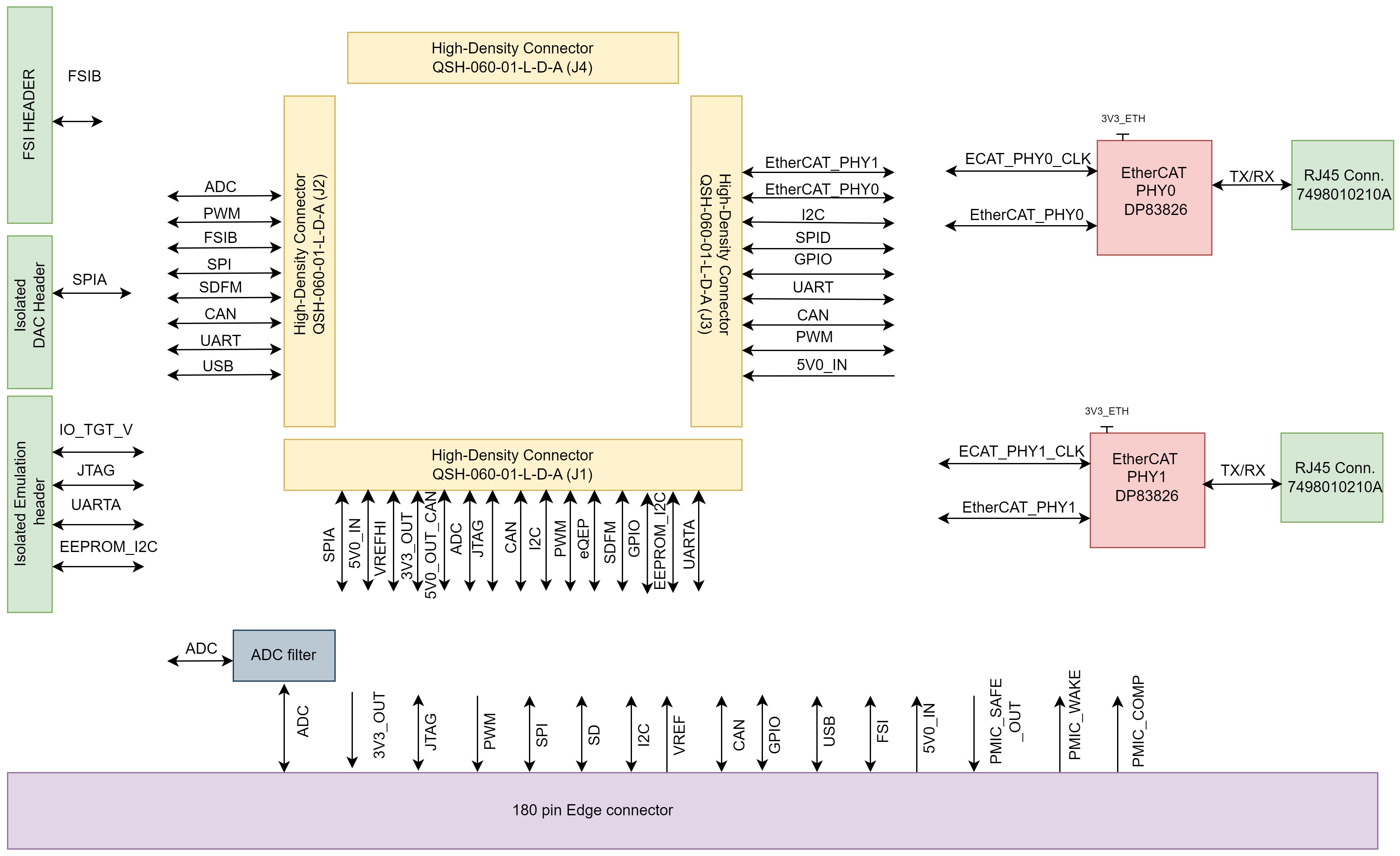
Figure 2-4
Block Diagram