SPNS240A October 2014 – June 2015 RM41L232
PRODUCTION DATA.
- 1Device Overview
- 2Revision History
- 3Device Comparison
-
4Terminal Configuration and Functions
- 4.1 PZ QFP Package Pinout (100-Pin)
- 4.2
Terminal Functions
- 4.2.1 High-End Timer (N2HET)
- 4.2.2 Enhanced Quadrature Encoder Pulse Modules (eQEP)
- 4.2.3 General-Purpose Input/Output (GPIO)
- 4.2.4 Controller Area Network Interface Modules (DCAN1, DCAN2)
- 4.2.5 Multibuffered Serial Peripheral Interface (MibSPI1)
- 4.2.6 Standard Serial Peripheral Interface (SPI2)
- 4.2.7 Local Interconnect Network Controller (LIN)
- 4.2.8 Multibuffered Analog-to-Digital Converter (MibADC)
- 4.2.9 System Module
- 4.2.10 Error Signaling Module (ESM)
- 4.2.11 Main Oscillator
- 4.2.12 Test/Debug Interface
- 4.2.13 Flash
- 4.2.14 Core Supply
- 4.2.15 I/O Supply
- 4.2.16 Core and I/O Supply Ground Reference
- 4.3 Output Multiplexing and Control
- 4.4 Special Multiplexed Options
-
5Specifications
- 5.1 Absolute Maximum Ratings
- 5.2 ESD Ratings
- 5.3 Power-On Hours (POH)
- 5.4 Recommended Operating Conditions
- 5.5 Switching Characteristics Over Recommended Operating Conditions for Clock Domains
- 5.6 Wait States Required
- 5.7 Power Consumption
- 5.8 Thermal Resistance Characteristics for PZ
- 5.9 Input/Output Electrical Characteristics
- 5.10 Output Buffer Drive Strengths
- 5.11 Input Timings
- 5.12 Output Timings
-
6System Information and Electrical Specifications
- 6.1 Voltage Monitor Characteristics
- 6.2 Power Sequencing and Power-On Reset
- 6.3 Warm Reset (nRST)
- 6.4 ARM Cortex-R4 CPU Information
- 6.5 Clocks
- 6.6 Clock Monitoring
- 6.7 Glitch Filters
- 6.8 Device Memory Map
- 6.9 Flash Memory
- 6.10 Flash Program and Erase Timings for Program Flash
- 6.11 Flash Program and Erase Timings for Data Flash
- 6.12 Tightly Coupled RAM Interface Module
- 6.13 Parity Protection for Accesses to peripheral RAMs
- 6.14 On-Chip SRAM Initialization and Testing
- 6.15 Vectored Interrupt Manager
- 6.16 Real-Time Interrupt Module
- 6.17 Error Signaling Module
- 6.18 Reset / Abort / Error Sources
- 6.19 Digital Windowed Watchdog
- 6.20 Debug Subsystem
-
7Peripheral Information and Electrical Specifications
- 7.1 Peripheral Legend
- 7.2 Multibuffered 12-Bit Analog-to-Digital Converter
- 7.3 General-Purpose Input/Output
- 7.4 Enhanced High-End Timer (N2HET)
- 7.5 Controller Area Network (DCAN)
- 7.6 Local Interconnect Network Interface (LIN)
- 7.7 Multibuffered / Standard Serial Peripheral Interface
- 7.8 Enhanced Quadrature Encoder (eQEP)
- 8Device and Documentation Support
- 9Mechanical Packaging and Orderable Addendum
7 Peripheral Information and Electrical Specifications
7.1 Peripheral Legend
Table 7-1 Peripheral Legend
| ABBREVIATION | FULL NAME |
|---|---|
| MibADC | Multibuffered Analog-to-Digital Converter |
| CCM-R4 | CPU Compare Module – Cortex-R4 |
| CRC | Cyclic Redundancy Check |
| DCAN | Controller Area Network |
| DCC | Dual Clock Comparator |
| ESM | Error Signaling Module |
| GIO | General-Purpose Input/Output |
| HTU | High-End Timer Transfer Unit |
| LIN | Local Interconnect Network |
| MibSPI | Multibuffered Serial Peripheral Interface |
| N2HET | Platform High-End Timer |
| RTI | Real-Time Interrupt Module |
| SCI | Serial Communications Interface |
| SPI | Serial Peripheral Interface |
| VIM | Vectored Interrupt Manager |
7.2 Multibuffered 12-Bit Analog-to-Digital Converter
The multibuffered A-to-D converter (MibADC) has a separate power bus for its analog circuitry that enhances the A-to-D performance by preventing digital switching noise on the logic circuitry which could be present on VSS and VCC from coupling into the A-to-D analog stage. All A-to-D specifications are given with respect to ADREFLO unless otherwise noted.
Table 7-2 MibADC Overview
| DESCRIPTION | VALUE |
|---|---|
| Resolution | 12 bits |
| Monotonic | Assured |
| Output conversion code | 00h to FFFh [00 for VAI ≤ ADREFLO; FFF for VAI ≥ ADREFHI] |
7.2.1 Features
- 12-bit resolution
- ADREFHI and ADREFLO pins (high and low reference voltages)
- Total Sample/Hold/Convert time: 600 ns Typical Minimum at 30 MHz ADCLK
- One memory region per conversion group is available (event, group 1, group 2)
- Allocation of channels to conversion groups is completely programmable
- Memory regions are serviced by interrupt
- Programmable interrupt threshold counter is available for each group
- Programmable magnitude threshold interrupt for each group for any one channel
- Option to read either 8-, or 10-, or 12-bit values from memory regions
- Single or continuous conversion modes
- Embedded self-test
- Embedded calibration logic
- Enhanced power-down mode
- Optional feature to automatically power down ADC core when no conversion is in progress
- External event pin (ADEVT) programmable as general-purpose I/O
7.2.2 Event Trigger Options
The ADC module supports three conversion groups: Event Group, Group1, and Group2. Each of these three groups can be configured to be hardware event-triggered. In that case, the application can select from among eight event sources to be the trigger for the conversions of a group.
7.2.2.1 MIBADC Event Trigger Hookup
Table 7-3 MIBADC Event Trigger Hookup
| EVENT NUMBER | SOURCE SELECT BITS For G1, G2, or EVENT (G1SRC[2:0], G2SRC[2:0], or EVSRC[2:0]) |
TRIGGER |
|---|---|---|
| 1 | 000 | ADEVT |
| 2 | 001 | N2HET[8] |
| 3 | 010 | N2HET[10] |
| 4 | 011 | RTI compare 0 interrupt |
| 5 | 100 | N2HET[12] |
| 6 | 101 | N2HET[14] |
| 7 | 110 | N2HET[17] |
| 8 | 111 | N2HET[19] |
NOTE
For ADEVT, N2HET trigger sources, the connection to the MibADC module trigger input is made from the output side of the input buffer. This way, a trigger condition can be generated either by configuring the function as output onto the pad, or by driving the function from an external trigger source as input. If the mux controller module is used to select different functionality instead of ADEVT or N2HET[x], care must be taken to disable these signals from triggering conversions; there is no multiplexing on input connections.
NOTE
For the RTI compare 0 interrupt source, the connection is made directly from the output of the RTI module. That is, the interrupt condition can be used as a trigger source even if the actual interrupt is not signaled to the CPU.
7.2.3 ADC Electrical and Timing Specifications
Table 7-4 MibADC Recommended Operating Conditions
| PARAMETER | MIN | MAX | UNIT | |
|---|---|---|---|---|
| ADREFHI | A-to-D high-voltage reference source | ADREFLO | VCCAD | V |
| ADREFLO | A-to-D low-voltage reference source | VSSAD | ADREFHI | V |
| VAI | Analog input voltage | ADREFLO | ADREFHI | V |
| IAIC | Analog input clamp current (VAI < VSSAD – 0.3 or VAI > VCCAD + 0.3) |
–2 | 2 | mA |
Table 7-5 MibADC Electrical Characteristics Over Full Ranges of Recommended Operating Conditions(1)
| PARAMETER | DESCRIPTION/CONDITIONS | MIN | TYP | MAX | UNIT | ||
|---|---|---|---|---|---|---|---|
| Rmux | Analog input mux on-resistance | See Figure 7-1 | 95 | 250 | Ω | ||
| Rsamp | ADC sample switch on-resistance | See Figure 7-1 | 60 | 250 | Ω | ||
| Cmux | Input mux capacitance | See Figure 7-1 | 7 | 16 | pF | ||
| Csamp | ADC sample capacitance | See Figure 7-1 | 8 | 13 | pF | ||
| IAIL | Analog off-state input leakage current | VCCAD = 3.6 V MAX | VSSAD < VIN < VSSAD + 100 mV | –300 | –1 | 200 | nA |
| VSSAD + 100 mV < VIN < VCCAD - 200 mV | –200 | –0.3 | 200 | ||||
| VCCAD - 200 mV < VIN < VCCAD | –200 | 1 | 500 | ||||
| IAOSB | Analog on-state input bias | VCCAD = 3.6 V MAX | VSSAD < VIN < VSSAD + 100 mV | –8 | 2 | µA | |
| VSSAD + 100 mV < VIN < VCCAD - 200 mV | –4 | 2 | |||||
| VCCAD - 200 mV < VIN < VCCAD | –4 | 12 | |||||
| IADREFHI | ADREFHI input current | ADREFHI = VCCAD, ADREFLO = VSSAD | 3 | mA | |||
| ICCAD | Static supply current | Normal operating mode | (2) | mA | |||
| ADC core in power-down mode | 5 | µA | |||||
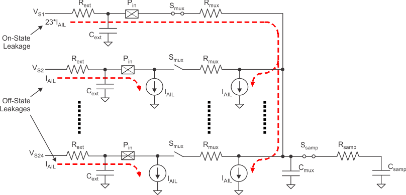 Figure 7-1 MibADC Input Equivalent Circuit
Table 7-6 MibADC Timing Specifications
| PARAMETER | MIN | NOM | MAX | UNIT | |
|---|---|---|---|---|---|
| tc(ADCLK)(2) | Cycle time, MibADC clock | 33 | ns | ||
| td(SH)(3) | Delay time, sample and hold time | 200 | ns | ||
| td(PU-ADV) | Delay time from ADC power on until first input can be sampled | 1 | µs | ||
| 12-BIT MODE | |||||
| td(C) | Delay time, conversion time | 400 | ns | ||
| td(SHC)(1) | Delay time, total sample/hold and conversion time | 600 | ns | ||
| 10-BIT MODE | |||||
| td(C) | Delay time, conversion time | 330 | ns | ||
| td(SHC)(1) | Delay time, total sample/hold and conversion time | 530 | ns | ||
Table 7-7 MibADC Operating Characteristics Over Full Ranges of Recommended Operating Conditions
| PARAMETER | DESCRIPTION/CONDITIONS | MIN | TYP | MAX | UNIT | |||
|---|---|---|---|---|---|---|---|---|
| CR | Conversion range over which specified accuracy is maintained | ADREFHI - ADREFLO | 3 | 3.6 | V | |||
| ZSET | Offset Error | Difference between the first ideal transition (from code 000h to 001h) and the actual transition | 10-bit mode | With ADC Calibration | 1 | LSB(1) | ||
| Without ADC Calibration | 2 | |||||||
| 12-bit mode | With ADC Calibration | 2 | ||||||
| Without ADC Calibration | 4 | |||||||
| FSET | Gain Error | Difference between the last ideal transition (from code FFEh to FFFh) and the actual transition minus offset. | 10-bit mode | 2 | LSB | |||
| 12-bit mode | 3 | |||||||
| EDNL | Differential nonlinearity error | Difference between the actual step width and the ideal value. (See Figure 7-2) |
10-bit mode | ± 1.5 | LSB | |||
| 12-bit mode | ± 2 | |||||||
| EINL | Integral nonlinearity error | Maximum deviation from the best straight line through the MibADC. MibADC transfer characteristics, excluding the quantization error. (See Figure 7-3) |
10-bit mode | ± 2 | LSB | |||
| 12-bit mode | ± 2 | |||||||
| ETOT | Total unadjusted error | Maximum value of the difference between an analog value and the ideal midstep value. (See Figure 7-4) | 10-bit mode | With ADC Calibration | ± 2 | LSB | ||
| Without ADC Calibration | ± 4 | |||||||
| 12-bit mode | With ADC Calibration | ± 4 | ||||||
| Without ADC Calibration | ± 7 | |||||||
7.2.4 Performance (Accuracy) Specifications
7.2.4.1 MibADC Nonlinearity Errors
The differential nonlinearity error shown in Figure 7-2 (sometimes referred to as differential linearity) is the difference between an actual step width and the ideal value of 1 LSB.
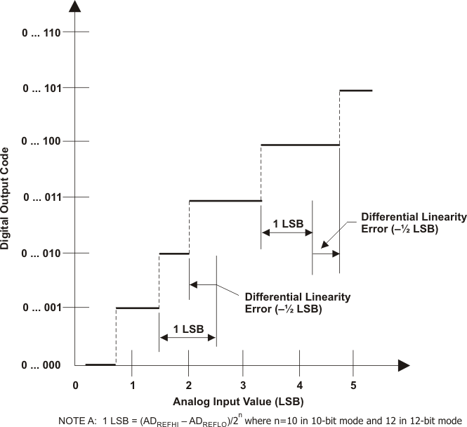 Figure 7-2 Differential Nonlinearity (DNL) Error
The integral nonlinearity error shown in Figure 7-3 (sometimes referred to as linearity error) is the deviation of the values on the actual transfer function from a straight line.
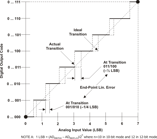 Figure 7-3 Integral Nonlinearity (INL) Error
7.2.4.2 MibADC Total Error
The absolute accuracy or total error of an MibADC as shown in Figure 7-4 is the maximum value of the difference between an analog value and the ideal midstep value.
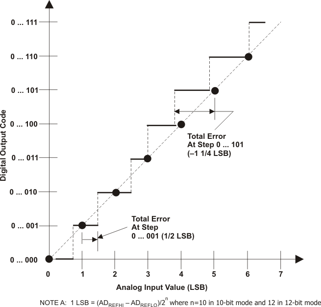 Figure 7-4 Absolute Accuracy (Total) Error
7.3 General-Purpose Input/Output
The GPIO module on this device supports one port GIOA. The I/O pins are bidirectional and bit-programmable. GIOA supports external interrupt capability.
7.3.1 Features
The GPIO module has the following features:
- Each I/O pin can be configured as:
- Input
- Output
- Open Drain
- The interrupts have the following characteristics:
- Programmable interrupt detection either on both edges or on a single edge (set in GIOINTDET)
- Programmable edge-detection polarity, either rising or falling edge (set in GIOPOL register)
- Individual interrupt flags (set in GIOFLG register)
- Individual interrupt enables, set and cleared through GIOENASET and GIOENACLR registers respectively
- Programmable interrupt priority, set through GIOLVLSET and GIOLVLCLR registers
- Internal pullup/pulldown allows unused I/O pins to be left unconnected
For information on input and output timings see Section 5.11 and Section 5.12
7.4 Enhanced High-End Timer (N2HET)
The N2HET is an advanced intelligent timer that provides sophisticated timing functions for real-time applications. The timer is software-controlled, using a reduced instruction set, with a specialized timer micromachine and an attached I/O port. The N2HET can be used for pulse width modulated outputs, capture or compare inputs, or general-purpose I/O.. It is especially well suited for applications requiring multiple sensor information and drive actuators with complex and accurate time pulses.
7.4.1 Features
The N2HET module has the following features:
- Programmable timer for input and output timing functions
- Reduced instruction set (30 instructions) for dedicated time and angle functions
- 128 words of instruction RAM protected by parity
- User defined number of 25-bit virtual counters for timer, event counters and angle counters
- 7-bit hardware counters for each pin allow up to 32-bit resolution in conjunction with the 25-bit virtual counters
- Up to 19 pins usable for input signal measurements or output signal generation
- Programmable suppression filter for each input pin with adjustable limiting frequency
- Low CPU overhead and interrupt load
- Efficient data transfer to or from the CPU memory with dedicated High-End-Timer Transfer Unit (HTU)
- Diagnostic capabilities with different loopback mechanisms and pin status readback functionality
7.4.2 N2HET RAM Organization
The timer RAM uses 4 RAM banks, where each bank has two port access capability. This means that one RAM address may be written while another address is read. The RAM words are 96-bits wide, which are split into three 32-bit fields (program, control, and data).
7.4.3 Input Timing Specifications
The N2HET instructions PCNT and WCAP impose some timing constraints on the input signals.
 Figure 7-5 N2HET Input Capture Timings
Table 7-8 Dynamic Characteristics for the N2HET Input Capture Functionality
| PARAMETER | MIN(1)(2) | MAX(1)(2) | UNIT | |
|---|---|---|---|---|
| 1 | Input signal period, PCNT or WCAP for rising edge to rising edge | (hr)(lr) tc(VCLK2) + 2 | 225(hr)(lr)tc(VCLK2) - 2 | ns |
| 2 | Input signal period, PCNT or WCAP for falling edge to falling edge | (hr) (lr) tc(VCLK2) + 2 | 225 (hr)(lr) tc(VCLK2) - 2 | ns |
| 3 | Input signal high phase, PCNT or WCAP for rising edge to falling edge | 2(hr) tc(VCLK2) + 2 | 225 (hr)(lr) tc(VCLK2) - 2 | ns |
| 4 | Input signal low phase, PCNT or WCAP for falling edge to rising edge | 2(hr) tc(VCLK2) + 2 | 225 (hr)(lr) tc(VCLK2) - 2 | ns |
7.4.4 N2HET Checking
7.4.4.1 Output Monitoring using Dual Clock Comparator (DCC)
N2HET[31] is connected as a clock source for counter 1 in DCC1. This allows the application to measure the frequency of the pulse-width modulated (PWM) signal on N2HET[31].
N2HET[31] can be configured to be an internal-only channel. That is, the connection to the DCC module is made directly from the output of the N2HET module (from the input of the output buffer).
For more information on DCC, see Section 6.6.3.
7.4.5 Disabling N2HET Outputs
Some applications require the N2HET outputs to be disabled under some fault condition. The N2HET module provides this capability through the "Pin Disable" input signal. This signal, when driven low, causes the N2HET outputs identified by a programmable register (HETPINDIS) to be tri-stated.
For more details on the "N2HET Pin Disable" feature, see the device-specific Technical Reference Manual listed in Section 8.2.1.
GIOA[5] and EQEPERR are connected to the "Pin Disable" input for N2HET. In the case of GIOA[5] connection, this connection is made from the output of the input buffer. In the case of EQEPERR, the EQEPERR output signal is asserted in the event of a phase error. This signal is inverted and double-synchronized to VCLK2 for input into the N2HET PIN_nDISABLE port.
The PIN_nDISABLE port input source is selectable between the GIOA[5] and EQEPERR sources. This is achieved through the PINMMR9[1:0] bits.
7.4.6 High-End Timer Transfer Unit (N2HET)
A High-End Timer Transfer Unit (N2HET) can perform DMA type transactions to transfer N2HET data to or from main memory. A Memory Protection Unit (MPU) is built into the N2HET.
7.4.6.1 Features
- CPU independent
- Master Port to access system memory
- 8 control packets supporting dual buffer configuration
- Control packet information is stored in RAM protected by parity
- Event synchronization (N2HET transfer requests)
- Supports 32- or 64-bit transactions
- Addressing modes for N2HET address (8 byte or 16 byte) and system memory address (fixed, 32-bit or 64-bit)
- One shot, circular, and auto switch buffer transfer modes
- Request lost detection
7.4.6.2 Trigger Connections
Table 7-9 N2HET Request Line Connection
| MODULES | REQUEST SOURCE | HTU REQUEST |
|---|---|---|
| N2HET | HTUREQ[0] | HTU DCP[0] |
| N2HET | HTUREQ[1] | HTU DCP[1] |
| N2HET | HTUREQ[2] | HTU DCP[2] |
| N2HET | HTUREQ[3] | HTU DCP[3] |
| N2HET | HTUREQ[4] | HTU DCP[4] |
| N2HET | HTUREQ[5] | HTU DCP[5] |
| N2HET | HTUREQ[6] | HTU DCP[6] |
| N2HET | HTUREQ[7] | HTU DCP[7] |
7.5 Controller Area Network (DCAN)
The DCAN supports the CAN 2.0B protocol standard and uses a serial, multimaster communication protocol that efficiently supports distributed real-time control with robust communication rates of up to 1 Mbps. The DCAN is ideal for applications operating in noisy and harsh environments (for example, automotive and industrial fields) that require reliable serial communication or multiplexed wiring.
7.5.1 Features
Features of the DCAN module include:
- Supports CAN protocol version 2.0 part A, B
- Bit rates up to 1 Mbps
- The CAN kernel can be clocked by the oscillator for baud-rate generation.
- 32 and 16 mailboxes on DCAN1 and DCAN2, respectively
- Individual identifier mask for each message object
- Programmable FIFO mode for message objects
- Programmable loop-back modes for self-test operation
- Automatic bus on after Bus-Off state by a programmable 32-bit timer
- Message RAM protected by parity
- Direct access to Message RAM during test mode
- CAN RX / TX pins configurable as general-purpose I/O pins
- Message RAM Auto Initialization
For more information on the DCAN, see the device-specific Technical Reference Manual listed in Section 8.2.1.
7.5.2 Electrical and Timing Specifications
Table 7-10 Dynamic Characteristics for the DCANx TX and RX pins
| PARAMETER | MIN | MAX | UNIT | |
|---|---|---|---|---|
| td(CANnTX) | Delay time, transmit shift register to CANnTX pin(1) | 15 | ns | |
| td(CANnRX) | Delay time, CANnRX pin to receive shift register | 5 | ns | |
7.6 Local Interconnect Network Interface (LIN)
The SCI/LIN module can be programmed to work either as an SCI or as a LIN. The core of the module is an SCI. The SCI’s hardware features are augmented to achieve LIN compatibility.
The SCI module is a universal asynchronous receiver-transmitter that implements the standard nonreturn to zero format. The SCI can be used to communicate, for example, through an RS-232 port or over a K-line.
The LIN standard is based on the SCI (UART) serial data link format. The communication concept is single-master/multiple-slave with a message identification for multicast transmission between any network nodes.
7.6.1 LIN Features
The following are features of the LIN module:
- Compatible to LIN 1.3, 2.0 and 2.1 protocols
- Multibuffered receive and transmit units
- Identification masks for message filtering
- Automatic Master Header Generation
- Programmable Synch Break Field
- Synch Field
- Identifier Field
- Slave Automatic Synchronization
- Synch break detection
- Optional baudrate update
- Synchronization Validation
- 231 programmable transmission rates with 7 fractional bits
- Error detection
- 2 Interrupt lines with priority encoding
7.7 Multibuffered / Standard Serial Peripheral Interface
The MibSPI is a high-speed synchronous serial input/output port that allows a serial bit stream of programmed length (2 to 16 bits) to be shifted in and out of the device at a programmed bit-transfer rate. Typical applications for the SPI include interfacing to external peripherals, such as I/Os, memories, display drivers, and ADCs.
7.7.1 Features
Both Standard and MibSPI modules have the following features:
- 16-bit shift register
- Receive buffer register
- 11-bit baud clock generator
- SPICLK can be internally generated (master mode) or received from an external clock source (slave mode)
- Each word transferred can have a unique format
- SPI I/Os not used in the communication can be used as digital input/output signals
Table 7-11 MibSPI/SPI Default Configurations
| MibSPIx/SPIx | I/Os |
|---|---|
| MibSPI1 | MIBSPI1SIMO[0], MIBSPI1SOMI[0], MIBSPI1CLK, MIBSPI1nCS[3:0], MIBSPI1nENA |
| SPI2 | SPI2SIMO, SPI2SOMI, SPI2CLK, SPI2nCS[0] |
| SPI3 | SPI3SIMO, SPI3SOMI, SPI3CLK, SPI3nENA, SPI3nCS[0] |
7.7.2 MibSPI Transmit and Receive RAM Organization
The Multibuffer RAM is comprised of 128 buffers. Each entry in the Multibuffer RAM consists of four parts: a 16-bit transmit field, a 16-bit receive field, a 16-bit control field, and a 16-bit status field. The Multibuffer RAM can be partitioned into multiple transfer group with variable number of buffers each.
7.7.3 MibSPI Transmit Trigger Events
Each of the transfer groups can be configured individually. For each of the transfer groups a trigger event and a trigger source can be chosen. A trigger event can be, for example, a rising edge or a permanent low level at a selectable trigger source. Up to 15 trigger sources are available which can be used by each transfer group. These trigger options are listed in Table 7-12.
7.7.3.1 MIBSPI1 Event Trigger Hookup
Table 7-12 MIBSPI1 Event Trigger Hookup
| EVENT NO. | TGxCTRL TRIGSRC[3:0] | TRIGGER |
|---|---|---|
| Disabled | 0000 | No trigger source |
| EVENT0 | 0001 | GIOA[0] |
| EVENT1 | 0010 | GIOA[1] |
| EVENT2 | 0011 | GIOA[2] |
| EVENT3 | 0100 | GIOA[3] |
| EVENT4 | 0101 | GIOA[4] |
| EVENT5 | 0110 | GIOA[5] |
| EVENT6 | 0111 | GIOA[6] |
| EVENT7 | 1000 | GIOA[7] |
| EVENT8 | 1001 | N2HET[8] |
| EVENT9 | 1010 | N2HET[10] |
| EVENT10 | 1011 | N2HET[12] |
| EVENT11 | 1100 | N2HET[14] |
| EVENT12 | 1101 | N2HET[16] |
| EVENT13 | 1110 | N2HET[18] |
| EVENT14 | 1111 | Internal Tick counter |
NOTE
For N2HET trigger sources, the connection to the MibSPI1 module trigger input is made from the input side of the output buffer (at the N2HET module boundary). This way, a trigger condition can be generated even if the N2HET signal is not selected to be output on the pad.
NOTE
For GIOx trigger sources, the connection to the MibSPI1 module trigger input is made from the output side of the input buffer. This way, a trigger condition can be generated either by selecting the GIOx pin as an output pin, or by driving the GIOx pin from an external trigger source.
7.7.4 MibSPI/SPI Master Mode I/O Timing Specifications
Table 7-13 SPI Master Mode External Timing Parameters (CLOCK PHASE = 0, SPICLK = output, SPISIMO = output, and SPISOMI = input)(1)(2)(3)
| NO. | PARAMETER | MIN | MAX | UNIT | ||
|---|---|---|---|---|---|---|
| 1 | tc(SPC)M | Cycle time, SPICLK(4) | 40 | 256tc(VCLK) | ns | |
| 2(5) | tw(SPCH)M | Pulse duration, SPICLK high (clock polarity = 0) | 0.5tc(SPC)M – tr(SPC)M – 3 | 0.5tc(SPC)M + 3 | ns | |
| tw(SPCL)M | Pulse duration, SPICLK low (clock polarity = 1) | 0.5tc(SPC)M – tf(SPC)M – 3 | 0.5tc(SPC)M + 3 | |||
| 3(5) | tw(SPCL)M | Pulse duration, SPICLK low (clock polarity = 0) | 0.5tc(SPC)M – tf(SPC)M – 3 | 0.5tc(SPC)M + 3 | ns | |
| tw(SPCH)M | Pulse duration, SPICLK high (clock polarity = 1) | 0.5tc(SPC)M – tr(SPC)M – 3 | 0.5tc(SPC)M + 3 | |||
| 4(5) | td(SPCH-SIMO)M | Delay time, SPISIMO valid before SPICLK low (clock polarity = 0) | 0.5tc(SPC)M – 6 | ns | ||
| td(SPCL-SIMO)M | Delay time, SPISIMO valid before SPICLK high (clock polarity = 1) | 0.5tc(SPC)M – 6 | ||||
| 5(5) | tv(SPCL-SIMO)M | Valid time, SPISIMO data valid after SPICLK low (clock polarity = 0) | 0.5tc(SPC)M – tf(SPC) – 4 | ns | ||
| tv(SPCH-SIMO)M | Valid time, SPISIMO data valid after SPICLK high (clock polarity = 1) | 0.5tc(SPC)M – tr(SPC) – 4 | ||||
| 6(5) | tsu(SOMI-SPCL)M | Setup time, SPISOMI before SPICLK low (clock polarity = 0) | tf(SPC) + 2.2 | ns | ||
| tsu(SOMI-SPCH)M | Setup time, SPISOMI before SPICLK high (clock polarity = 1) | tr(SPC) + 2.2 | ||||
| 7(5) | th(SPCL-SOMI)M | Hold time, SPISOMI data valid after SPICLK low (clock polarity = 0) | 10 | ns | ||
| th(SPCH-SOMI)M | Hold time, SPISOMI data valid after SPICLK high (clock polarity = 1) | 10 | ||||
| 8(6) | tC2TDELAY | Setup time CS active until SPICLK high (clock polarity = 0) | CSHOLD = 0 | C2TDELAY*tc(VCLK) + 2*tc(VCLK) - tf(SPICS) + tr(SPC) – 7 | (C2TDELAY+2) * tc(VCLK) - tf(SPICS) + tr(SPC) + 5.5 | ns |
| CSHOLD = 1 | C2TDELAY*tc(VCLK) + 3*tc(VCLK) - tf(SPICS) + tr(SPC) – 7 | (C2TDELAY+3) * tc(VCLK) - tf(SPICS) + tr(SPC) + 5.5 | ||||
| Setup time CS active until SPICLK low (clock polarity = 1) | CSHOLD = 0 | C2TDELAY*tc(VCLK) + 2*tc(VCLK) - tf(SPICS) + tf(SPC) – 7 | (C2TDELAY+2) * tc(VCLK) - tf(SPICS) + tf(SPC) + 5.5 | ns | ||
| CSHOLD = 1 | C2TDELAY*tc(VCLK) + 3*tc(VCLK) - tf(SPICS) + tf(SPC) – 7 | (C2TDELAY+3) * tc(VCLK) - tf(SPICS) + tf(SPC) + 5.5 | ||||
| 9(6) | tT2CDELAY | Hold time SPICLK low until CS inactive (clock polarity = 0) | 0.5*tc(SPC)M + T2CDELAY*tc(VCLK) + tc(VCLK) - tf(SPC) + tr(SPICS) - 7 | 0.5*tc(SPC)M + T2CDELAY*tc(VCLK) + tc(VCLK) - tf(SPC) + tr(SPICS) + 11 | ns | |
| Hold time SPICLK high until CS inactive (clock polarity = 1) | 0.5*tc(SPC)M + T2CDELAY*tc(VCLK) + tc(VCLK) - tr(SPC) + tr(SPICS) - 7 | 0.5*tc(SPC)M + T2CDELAY*tc(VCLK) + tc(VCLK) - tr(SPC) + tr(SPICS) + 11 | ns | |||
| 10 | tSPIENA | SPIENAn Sample point | (C2TDELAY+1) * tc(VCLK) - tf(SPICS) – 29 | (C2TDELAY+1)*tc(VCLK) | ns | |
| 11 | tSPIENAW | SPIENAn Sample point from write to buffer | (C2TDELAY+2)*tc(VCLK) | ns | ||
For PS values from 1 to 255: tc(SPC)M ≥ (PS +1)tc(VCLK) ≥ 40 ns, where PS is the prescale value set in the SPIFMTx.[15:8] register bits.
For PS values of 0: tc(SPC)M = 2tc(VCLK) ≥ 40 ns.
The external load on the SPICLK pin must be less than 60 pF.
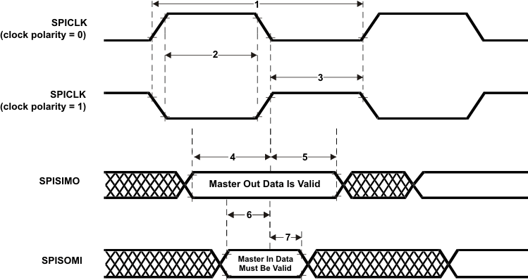 Figure 7-6 SPI Master Mode External Timing (CLOCK PHASE = 0)
 Figure 7-7 SPI Master Mode Chip Select Timing (CLOCK PHASE = 0)
Table 7-14 SPI Master Mode External Timing Parameters (CLOCK PHASE = 1, SPICLK = output, SPISIMO = output, and SPISOMI = input)(1)(2)(3)
| NO. | PARAMETER | MIN | MAX | UNIT | ||
|---|---|---|---|---|---|---|
| 1 | tc(SPC)M | Cycle time, SPICLK (4) | 40 | 256tc(VCLK) | ns | |
| 2(5) | tw(SPCH)M | Pulse duration, SPICLK high (clock polarity = 0) | 0.5tc(SPC)M – tr(SPC)M – 3 | 0.5tc(SPC)M + 3 | ns | |
| tw(SPCL)M | Pulse duration, SPICLK low (clock polarity = 1) | 0.5tc(SPC)M – tf(SPC)M – 3 | 0.5tc(SPC)M + 3 | |||
| 3(5) | tw(SPCL)M | Pulse duration, SPICLK low (clock polarity = 0) | 0.5tc(SPC)M – tf(SPC)M – 3 | 0.5tc(SPC)M + 3 | ns | |
| tw(SPCH)M | Pulse duration, SPICLK high (clock polarity = 1) | 0.5tc(SPC)M – tr(SPC)M – 3 | 0.5tc(SPC)M + 3 | |||
| 4(5) | tv(SIMO-SPCH)M | Valid time, SPICLK high after SPISIMO data valid (clock polarity = 0) | 0.5tc(SPC)M – 6 | ns | ||
| tv(SIMO-SPCL)M | Valid time, SPICLK low after SPISIMO data valid (clock polarity = 1) | 0.5tc(SPC)M – 6 | ||||
| 5(5) | tv(SPCH-SIMO)M | Valid time, SPISIMO data valid after SPICLK high (clock polarity = 0) | 0.5tc(SPC)M – tr(SPC) – 4 | ns | ||
| tv(SPCL-SIMO)M | Valid time, SPISIMO data valid after SPICLK low (clock polarity = 1) | 0.5tc(SPC)M – tf(SPC) – 4 | ||||
| 6(5) | tsu(SOMI-SPCH)M | Setup time, SPISOMI before SPICLK high (clock polarity = 0) | tr(SPC) + 2.2 | ns | ||
| tsu(SOMI-SPCL)M | Setup time, SPISOMI before SPICLK low (clock polarity = 1) | tf(SPC) + 2.2 | ||||
| 7(5) | tv(SPCH-SOMI)M | Valid time, SPISOMI data valid after SPICLK high (clock polarity = 0) | 10 | ns | ||
| tv(SPCL-SOMI)M | Valid time, SPISOMI data valid after SPICLK low (clock polarity = 1) | 10 | ||||
| 8(6) | tC2TDELAY | Setup time CS active until SPICLK high (clock polarity = 0) | CSHOLD = 0 | 0.5*tc(SPC)M + (C2TDELAY+2) * tc(VCLK) - tf(SPICS) + tr(SPC) – 7 | 0.5*tc(SPC)M + (C2TDELAY+2) * tc(VCLK) - tf(SPICS) + tr(SPC) + 5.5 | ns |
| CSHOLD = 1 | 0.5*tc(SPC)M + (C2TDELAY+3) * tc(VCLK) - tf(SPICS) + tr(SPC) – 7 | 0.5*tc(SPC)M + (C2TDELAY+3) * tc(VCLK) - tf(SPICS) + tr(SPC) + 5.5 | ||||
| Setup time CS active until SPICLK low (clock polarity = 1) | CSHOLD = 0 | 0.5*tc(SPC)M + (C2TDELAY+2) * tc(VCLK) - tf(SPICS) + tf(SPC) – 7 | 0.5*tc(SPC)M + (C2TDELAY+2) * tc(VCLK) - tf(SPICS) + tf(SPC) + 5.5 | ns | ||
| CSHOLD = 1 | 0.5*tc(SPC)M + (C2TDELAY+3) * tc(VCLK) - tf(SPICS) + tf(SPC) – 7 | 0.5*tc(SPC)M + (C2TDELAY+3) * tc(VCLK) - tf(SPICS) + tf(SPC) + 5.5 | ||||
| 9(6) | tT2CDELAY | Hold time SPICLK low until CS inactive (clock polarity = 0) | T2CDELAY*tc(VCLK) + tc(VCLK) - tf(SPC) + tr(SPICS) - 7 | T2CDELAY*tc(VCLK) + tc(VCLK) - tf(SPC) + tr(SPICS) + 11 | ns | |
| Hold time SPICLK high until CS inactive (clock polarity = 1) | T2CDELAY*tc(VCLK) + tc(VCLK) - tr(SPC) + tr(SPICS) - 7 | T2CDELAY*tc(VCLK) + tc(VCLK) - tr(SPC) + tr(SPICS) + 11 | ns | |||
| 10 | tSPIENA | SPIENAn Sample Point | (C2TDELAY+1)* tc(VCLK) - tf(SPICS) – 29 | (C2TDELAY+1)*tc(VCLK) | ns | |
| 11 | tSPIENAW | SPIENAn Sample point from write to buffer | (C2TDELAY+2)*tc(VCLK) | ns | ||
For PS values from 1 to 255: tc(SPC)M ≥ (PS +1)tc(VCLK) ≥ 40 ns, where PS is the prescale value set in the SPIFMTx.[15:8] register bits.
For PS values of 0: tc(SPC)M = 2tc(VCLK) ≥ 40 ns.
The external load on the SPICLK pin must be less than 60 pF.
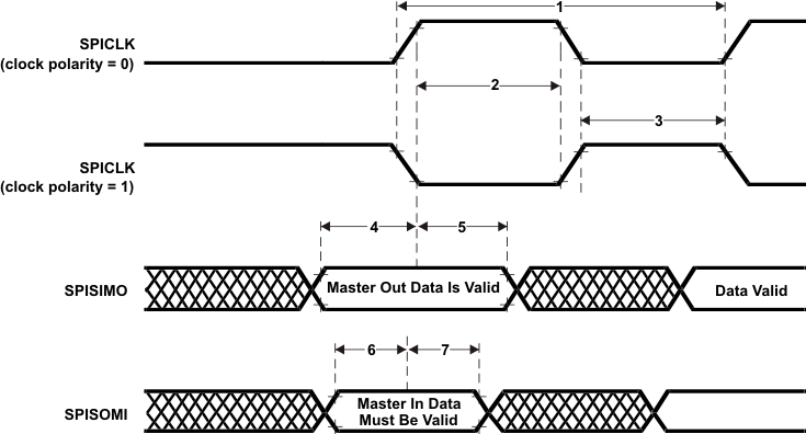 Figure 7-8 SPI Master Mode External Timing (CLOCK PHASE = 1)
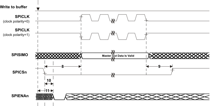 Figure 7-9 SPI Master Mode Chip Select Timing (CLOCK PHASE = 1)
7.7.5 SPI Slave Mode I/O Timings
Table 7-15 SPI Slave Mode External Timing Parameters (CLOCK PHASE = 0, SPICLK = input, SPISIMO = input, and SPISOMI = output)(1)(2)(3)(4)
| NO. | PARAMETER | MIN | MAX | UNIT | |
|---|---|---|---|---|---|
| 1 | tc(SPC)S | Cycle time, SPICLK(5) | 40 | ns | |
| 2(6) | tw(SPCH)S | Pulse duration, SPICLK high (clock polarity = 0) | 14 | ns | |
| tw(SPCL)S | Pulse duration, SPICLK low (clock polarity = 1) | 14 | |||
| 3(6) | tw(SPCL)S | Pulse duration, SPICLK low (clock polarity = 0) | 14 | ns | |
| tw(SPCH)S | Pulse duration, SPICLK high (clock polarity = 1) | 14 | |||
| 4(6) | td(SPCH-SOMI)S | Delay time, SPISOMI valid after SPICLK high (clock polarity = 0) | trf(SOMI) + 20 | ns | |
| td(SPCL-SOMI)S | Delay time, SPISOMI valid after SPICLK low (clock polarity = 1) | trf(SOMI) + 20 | |||
| 5(6) | th(SPCH-SOMI)S | Hold time, SPISOMI data valid after SPICLK high (clock polarity =0) | 2 | ns | |
| th(SPCL-SOMI)S | Hold time, SPISOMI data valid after SPICLK low (clock polarity =1) | 2 | |||
| 6(6) | tsu(SIMO-SPCL)S | Setup time, SPISIMO before SPICLK low (clock polarity = 0) | 4 | ns | |
| tsu(SIMO-SPCH)S | Setup time, SPISIMO before SPICLK high (clock polarity = 1) | 4 | |||
| 7(6) | th(SPCL-SIMO)S | Hold time, SPISIMO data valid after SPICLK low (clock polarity = 0) | 2 | ns | |
| th(SPCH-SIMO)S | Hold time, SPISIMO data valid after S PICLK high (clock polarity = 1) | 2 | |||
| 8 | td(SPCL-SENAH)S | Delay time, SPIENAn high after last SPICLK low (clock polarity = 0) | 1.5tc(VCLK) | 2.5tc(VCLK)+tr(ENAn)+ 22 | ns |
| td(SPCH-SENAH)S | Delay time, SPIENAn high after last SPICLK high (clock polarity = 1) | 1.5tc(VCLK) | 2.5tc(VCLK)+ tr(ENAn) + 22 | ||
| 9 | td(SCSL-SENAL)S | Delay time, SPIENAn low after SPICSn low (if new data has been written to the SPI buffer) | tf(ENAn) | tc(VCLK)+tf(ENAn)+27 | ns |
For PS values from 1 to 255: tc(SPC)S ≥ (PS +1)tc(VCLK) ≥ 40 ns, where PS is the prescale value set in the SPIFMTx.[15:8] register bits.
For PS values of 0: tc(SPC)S = 2tc(VCLK) ≥ 40 ns.
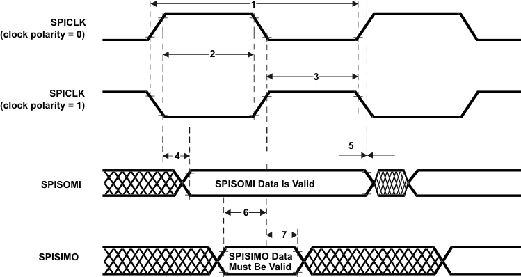 Figure 7-10 SPI Slave Mode External Timing (CLOCK PHASE = 0)
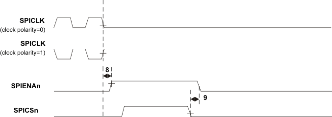 Figure 7-11 SPI Slave Mode Enable Timing (CLOCK PHASE = 0)
Table 7-16 SPI Slave Mode External Timing Parameters (CLOCK PHASE = 1, SPICLK = input, SPISIMO = input, and SPISOMI = output)(1)(2)(3)(4)
| NO. | PARAMETER | MIN | MAX | UNIT | |
|---|---|---|---|---|---|
| 1 | tc(SPC)S | Cycle time, SPICLK(5) | 40 | ns | |
| 2(6) | tw(SPCH)S | Pulse duration, SPICLK high (clock polarity = 0) | 14 | ns | |
| tw(SPCL)S | Pulse duration, SPICLK low (clock polarity = 1) | 14 | |||
| 3(6) | tw(SPCL)S | Pulse duration, SPICLK low (clock polarity = 0) | 14 | ns | |
| tw(SPCH)S | Pulse duration, SPICLK high (clock polarity = 1) | 14 | |||
| 4(6) | td(SOMI-SPCL)S | Dealy time, SPISOMI data valid after SPICLK low (clock polarity = 0) | trf(SOMI) + 20 | ns | |
| td(SOMI-SPCH)S | Delay time, SPISOMI data valid after SPICLK high (clock polarity = 1) | trf(SOMI) + 20 | |||
| 5(6) | th(SPCL-SOMI)S | Hold time, SPISOMI data valid after SPICLK high (clock polarity =0) | 2 | ns | |
| th(SPCH-SOMI)S | Hold time, SPISOMI data valid after SPICLK low (clock polarity =1) | 2 | |||
| 6(6) | tsu(SIMO-SPCH)S | Setup time, SPISIMO before SPICLK high (clock polarity = 0) | 4 | ns | |
| tsu(SIMO-SPCL)S | Setup time, SPISIMO before SPICLK low (clock polarity = 1) | 4 | |||
| 7(6) | tv(SPCH-SIMO)S | High time, SPISIMO data valid after SPICLK high (clock polarity = 0) | 2 | ns | |
| tv(SPCL-SIMO)S | High time, SPISIMO data valid after SPICLK low (clock polarity = 1) | 2 | |||
| 8 | td(SPCH-SENAH)S | Delay time, SPIENAn high after last SPICLK high (clock polarity = 0) | 1.5tc(VCLK) | 2.5tc(VCLK)+tr(ENAn) + 22 | ns |
| td(SPCL-SENAH)S | Delay time, SPIENAn high after last SPICLK low (clock polarity = 1) | 1.5tc(VCLK) | 2.5tc(VCLK)+tr(ENAn) + 22 | ||
| 9 | td(SCSL-SENAL)S | Delay time, SPIENAn low after SPICSn low (if new data has been written to the SPI buffer) | tf(ENAn) | tc(VCLK)+tf(ENAn)+ 27 | ns |
| 10 | td(SCSL-SOMI)S | Delay time, SOMI valid after SPICSn low (if new data has been written to the SPI buffer) | tc(VCLK) | 2tc(VCLK)+trf(SOMI)+ 28 | ns |
For PS values from 1 to 255: tc(SPC)S ≥ (PS +1)tc(VCLK) ≥ 40 ns, where PS is the prescale value set in the SPIFMTx.[15:8] register bits.
For PS values of 0: tc(SPC)S = 2tc(VCLK) ≥ 40 ns.
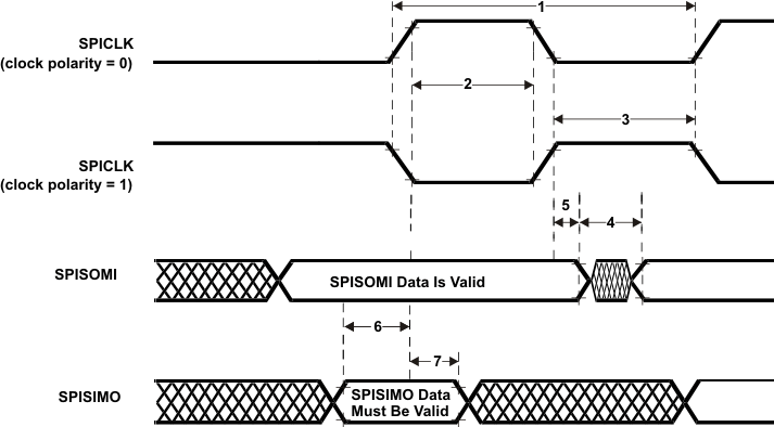 Figure 7-12 SPI Slave Mode External Timing (CLOCK PHASE = 1)
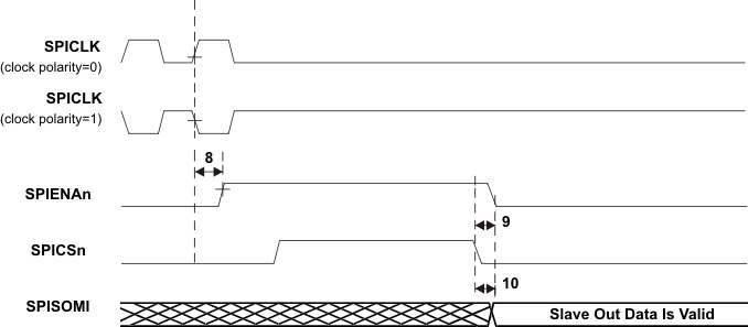 Figure 7-13 SPI Slave Mode Enable Timing (CLOCK PHASE = 1)
7.8 Enhanced Quadrature Encoder (eQEP)
Figure 7-14 shows the eQEP module interconnections on the device.
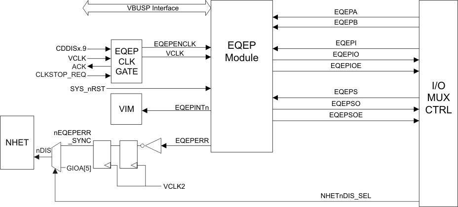 Figure 7-14 eQEP Module Interconnections
7.8.1 Clock Enable Control for eQEPx Modules
The device level control of the eQEP clock is accomplished through the enable/disable of the VCLK clock domain for eQEP only. This is realized using bit 9 of the CLKDDIS register. The eQEP clock source is enabled by default.
7.8.2 Using eQEPx Phase Error
The eQEP module sets the EQEPERR signal output whenever a phase error is detected in its inputs EQEPxA and EQEPxB. This error signal from both the eQEP modules is input to the connection selection multiplexor. As shown in Figure 7-14, the output of this selection multiplexor is inverted and connected to the N2HET module. This connection allows the application to define the response to a phase error indicated by the eQEP modules.
7.8.3 Input Connections to eQEPx Modules
The input connections to each of the eQEP modules can be selected between a double-VCLK-synchronized input or a double-VCLK-synchronized and filtered input, as shown in Table 7-17.
Table 7-17 Device-Level Input Synchronization
| INPUT SIGNAL | CONTROL FOR DOUBLE-SYNCHRONIZED CONNECTION TO eQEPx |
CONTROL FOR DOUBLE-SYNCHRONIZED AND FILTERED CONNECTION TO eQEPx |
|---|---|---|
| eQEPA | PINMMR8[0] = 1 | PINMMR8[0] = 0 and PINMMR8[1] = 1 |
| eQEPB | PINMMR8[8] = 1 | PINMMR8[8] = 0 and PINMMR8[9] = 1 |
| eQEPI | PINMMR8[16] = 1 | PINMMR8[16] = 0 and PINMMR8[17] = 1 |
| eQEPS | PINMMR8[24] = 1 | PINMMR8[24] = 0 and PINMMR8[25] = 1 |
7.8.4 Enhanced Quadrature Encoder Pulse (eQEPx) Timing
Table 7-18 eQEPx Timing Requirements
| PARAMETER | TEST CONDITIONS | MIN | MAX | UNIT | |
|---|---|---|---|---|---|
| tw(QEPP) | QEP input period | Synchronous | 2 tc(VCLK) | cycles | |
| Synchronous, with input filter | 2 tc(VCLK) + filter width | cycles | |||
| tw(INDEXH) | QEP Index Input High Time | Synchronous | 2 tc(VCLK) | cycles | |
| Synchronous, with input filter | 2 tc(VCLK) + filter width | cycles | |||
| tw(INDEXL) | QEP Index Input Low Time | Synchronous | 2 tc(VCLK) | cycles | |
| Synchronous, with input filter | 2 tc(VCLK) + filter width | cycles | |||
| tw(STROBH) | QEP Strobe Input High Time | Synchronous | 2 tc(VCLK) | cycles | |
| Synchronous, with input filter | 2 tc(VCLK) + filter width | cycles | |||
| tw(STROBL) | QEP Strobe Input Low Time | Synchronous | 2 tc(VCLK) | cycles | |
| Synchronous, with input filter | 2 tc(VCLK) + filter width | cycles | |||
Table 7-19 eQEPx Switching Characteristics
| PARAMETER | MIN | MAX | UNIT | |
|---|---|---|---|---|
| td(CNTR)xin | Delay time, external clock to counter increment | 4 tc(VCLK) | cycles | |
| td(PCS-OUT)QEP | Delay time, QEP input edge to position compare sync output | 6 tc(VCLK) | cycles | |