SPRAAV1C May 2009 – March 2020 AM3703 , AM3715 , OMAP3503 , OMAP3515 , OMAP3525 , OMAP3530
-
PCB Design Guidelines for 0.4mm Package-On-Package (PoP) Packages, Part I
- Trademarks
- 1 Using This Guide
- 2 A Word of Caution
- 3 A Team Sport
- 4 Be Wary of Quotes
- 5 Don’t Forget Your CAD Tools
- 6 Metric Vs English
- 7 PCB Fab Limits
- 8 Routing and Layer Stackup
- 9 OMAP35x 0.4mm Pitch
- 10 Pad Type
- 11 PCB Pad Dimensions for 0.4mm BGA Package
- 12 Multiple BGA Packages
- 13 Etch Traps and Heat Sinks
- 14 Vias and VIP
- 15 Laser Blind Vias
- 16 Filled Vias
- 17 Know Your Tools
- 18 BeagleBoard
- 19 BeagleBoard Views
- 20 OMAP35x Decoupling
- 21 PCB Finishes for High Density Interconnect (HDI)
- 22 Real World Second Opinion
- 23 Acknowledgments
- 24 References
- Revision History
22 Real World Second Opinion
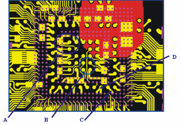
Our first OMAP35x EVM circuit board was designed prior to the release of these guidelines and was submitted to an assembly house. Elcotech, where they performed a DFM analysis on the gerber files. Below are their comments and Figure 26 shows this first pass at the EVM layout.
 Figure 26. First Pass DFM of the OMAP35x EVM
 This demonstrates how important good communication is between all members of the design team. Had this board gone into production, the yield would have been very poor. Our thanks to Elcoteq in Richardson, TX for their analysis from which this section was created. The list below has their comments tied to the various locations annotated in Figure 26.
- At location A, seven BGA Pads are ganged together. This acts as a large heatsink during reflow.
- The traces between D and the BGA pad should be narrower. A trace entering a pad should never be larger than the diameter of the pad.
- In some cases the BGA to ground plane is done like D and other it is done like A. Neither are good techniques.
- In C, the trace width exiting the BGA pad is much too large. In this case the trace acts as a heatsink during reflow.
- As in details A,B,C and D, the heat transfer from the ground planes is passing through a large via through a large trace and fanned out across 7 BGA pads ganged together.
- Do not gang BGA pads together with a copper plane as this increases the heat sink effect.