SPRABI1D January 2018 – July 2022 66AK2E05 , 66AK2G12 , 66AK2H06 , 66AK2H12 , 66AK2H14 , 66AK2L06 , AM5K2E02 , AM5K2E04 , SM320C6678-HIREL , TMS320C6652 , TMS320C6654 , TMS320C6655 , TMS320C6657 , TMS320C6670 , TMS320C6671 , TMS320C6672 , TMS320C6674 , TMS320C6678
- Trademarks
- 1 Introduction
- 2 Background
- 3 Migrating Designs From DDR2 to DDR3 (Features and Comparisons)
- 4 Prerequisites
- 5 Package Selection
-
6 Physical Design and Implementation
- 6.1 Electrical Connections
- 6.2 Signal Terminations
- 6.3
Mechanical Layout and Routing Considerations
- 6.3.1
Routing Considerations – SDRAMs
- 6.3.1.1 Mechanical Layout – SDRAMs
- 6.3.1.2 Stack Up – SDRAMs
- 6.3.1.3 Routing Rules – General Overview (SDRAMs)
- 6.3.1.4 Routing Rules – Address and Command Lines (SDRAMs)
- 6.3.1.5 Routing Rules – Control Lines (SDRAMs)
- 6.3.1.6 Routing Rules – Data Lines (SDRAMs)
- 6.3.1.7 Routing Rules – Clock Lines (SDRAMs)
- 6.3.1.8 Routing Rules – Power (SDRAMs)
- 6.3.1.9 Write Leveling Limit Impact on Routing – KeyStone I
- 6.3.1.10 Round-Trip Delay Impact on Routing – KeyStone I
- 6.3.1.11 Write Leveling Limit Impact on Routing – KeyStone II
- 6.3.1.12 Round-Trip Delay Impact on Routing – KeyStone II
- 6.3.2
Routing Considerations – UDIMMs
- 6.3.2.1 Mechanical Layout – UDIMMs
- 6.3.2.2 Stack Up – UDIMMs
- 6.3.2.3 Routing Rules – General Overview (UDIMMs)
- 6.3.2.4 Routing Rules – Address and Command Lines (UDIMMs)
- 6.3.2.5 Routing Rules – Control Lines (UDIMMs)
- 6.3.2.6 Routing Rules – Data Lines (UDIMMs)
- 6.3.2.7 Routing Rules – Clock Lines (UDIMMs)
- 6.3.2.8 Routing Rules – Power (UDIMMs)
- 6.3.2.9 Write-Leveling Limit Impact on Routing
- 6.3.1
Routing Considerations – SDRAMs
- 6.4 Timing Considerations
- 6.5 Impedance Considerations
- 6.6 Switching and Output Considerations
- 7 Simulation and Modeling
- 8 Power
- 9 Disclaimers
- 10References
- 11Revision History
4.7.2 Overshoot and Undershoot Specifications
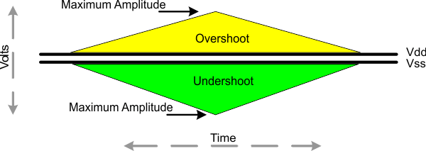
Overshoot (OS) and undershoot (US) limitations are defined in the following tables and figures. A theoretical instantaneous maximum upper and lower amplitude limit of 400 mV is allowed for overshoots and undershoots (assuming zero time is involved). Because each overshoot and undershoot has a component of time, each applicable signal must be further independently evaluated. Table 4-6 shows the limitations as listed in the current released standard for all address and control signals. Measurements are obtained at the pin of the memory DRAM and not the DSP.
| Speed | Max pk OS Amplitude (V) | Max pk US Amplitude (V) | Max OS Area Above VDD (V-ns) | Max US Area Below VSS (V-ns) |
|---|---|---|---|---|
| DDR3-800 | 0.4 | 0.4 | 0.67 | 0.67 |
| DDR3-1066 | 0.4 | 0.4 | 0.5 | 0.5 |
| DDR3-1333 | 0.4 | 0.4 | 0.4 | 0.4 |
| DDR3-1600 | 0.4 | 0.4 | 0.33 | 0.33 |
Figure 4-1 shows the limitations as listed in the current released standard for all address and control pins.
 Figure 4-1 Control and Address Overshoot
and Undershoot Requirements
Figure 4-1 Control and Address Overshoot
and Undershoot RequirementsTable 4-7 shows the limitations as listed in the current released standard for all data, clock, strobe, and mask signals.
| Speed | Max pk OS Amplitude (V) | Max pk US Amplitude (V) | Max OS Area Above VDD (V-ns) | Max US Area Below VSS (V-ns) |
|---|---|---|---|---|
| DDR3-800 | 0.4 | 0.4 | 0.25 | 0.25 |
| DDR3-1066 | 0.4 | 0.4 | 0.19 | 0.19 |
| DDR3-1333 | 0.4 | 0.4 | 0.15 | 0.15 |
| DDR3-1600 | 0.4 | 0.4 | 0.13 | 0.13 |
Figure 4-2 shows the limitations as listed in the current released standard for all data, clock, strobe, and mask signals.
 Figure 4-2 Data, Clock, Strobe, and Mask
Overshoot and Undershoot Requirements