SPRAC94D September   2018  – March 2022 AFE030 , AFE031 , TMS320F28075 , TMS320F28075-Q1 , TMS320F28076 , TMS320F28374D , TMS320F28374S , TMS320F28375D , TMS320F28375S , TMS320F28375S-Q1 , TMS320F28376D , TMS320F28376S , TMS320F28377D , TMS320F28377D-EP , TMS320F28377D-Q1 , TMS320F28377S , TMS320F28377S-Q1 , TMS320F28379D , TMS320F28379D-Q1 , TMS320F28379S


  1.   Trademarks
  2. FSK Overview
  3. Hardware Overview
    1. 2.1 Block Diagram
    2. 2.2 Hardware Setup
  4. Interfacing With the AFE03x
    1. 3.1 Configuring the AFE031
  5. Transmit Path
    1. 4.1 FSK Example Specifications
    2. 4.2 PWM Mode
      1. 4.2.1 Software Implementation
      2. 4.2.2 Testing Results
      3. 4.2.3 HRPWM vs. EPWM
    3. 4.3 DAC Mode
      1. 4.3.1 Software Implementation
      2. 4.3.2 Testing Results
      3. 4.3.3 OFDM Ability
    4. 4.4 Porting TX to LAUNCHXL-F280049C
      1. 4.4.1 PWM Mode Specific Porting
      2. 4.4.2 DAC Mode Specific Porting
  6. Receive Path
    1. 5.1 Receive Path Overview
    2. 5.2 Receiver Software Implementation
      1. 5.2.1 Initial Setup and Parameters
      2. 5.2.2 Interrupt Service Routines
      3. 5.2.3 Run Time Operation
      4. 5.2.4 Testing Results
      5. 5.2.5 System Utilization
      6. 5.2.6 Device Dependency and Porting
    3. 5.3 Tuning and Calibration
      1. 5.3.1 Setting the AFE03X's PGAs
      2. 5.3.2 Automatic Gain Control (AGC)
      3. 5.3.3 Setting the Bit Detection Threshold
      4. 5.3.4 FSK Correlation Detector Library
    4. 5.4 Porting RX to LAUNCHXL-F280049C
  7. Interfacing With a Power Line
    1. 6.1 Line Coupling
    2. 6.2 Coupling to an AC Line
      1. 6.2.1 Low Voltage Capacitor
      2. 6.2.2 The Ratio of the Transformer
      3. 6.2.3 HV Capacitor
      4. 6.2.4 HV Side Inductor
    3. 6.3 Coupling to DC Line
    4. 6.4 Protection Circuit
      1. 6.4.1 Metal Oxide Varistors
      2. 6.4.2 Transient Voltage Suppressors
      3. 6.4.3 Current Steering Diodes
    5. 6.5 Determining PA Power Supply Requirements
  8. Summary
  9. References
  10. Schematics
    1. 9.1 Schematics (PWM Mode)
    2. 9.2 Schematics (DAC Mode)
  11. 10Revision History

Block Diagram

Figure 2-3 shows a block diagram of the system. In this example, not all of the connections have been utilized, but all are present on the BoosterPack for future development.
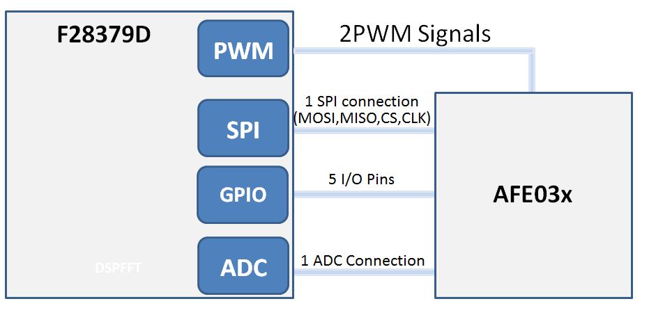
GUID-EBF9E7BD-34E1-4BD3-AD37-9DFD4908DCC4-low.jpgFigure 2-3 C2000 and AFE031 Block Diagram

The AFE has multiple internal registers that allow configuration of the internal components of the AFE chip, including filter selection, gain selection, and mode selections. These registers can be accessed using the SPI peripheral.

The AFE also has various GPIOs that allow the MCU to set the AFE into certain modes, as well as receive interrupts for critical events on the AFE. The ADC connection allows the MCU to receive or sample an input signal. The PWM signals provide a way to create an output for the AFE. Currently the AFE031 supports two modes of data transmission, PWM mode and DAC mode. An explanation and implementation of both of these modes can be found in Section 3.