SPRACK2A September 2019 – March 2020 TMS320F280021 , TMS320F280021-Q1 , TMS320F280023 , TMS320F280023-Q1 , TMS320F280023C , TMS320F280025 , TMS320F280025-Q1 , TMS320F280025C , TMS320F280025C-Q1 , TMS320F280040-Q1 , TMS320F280040C-Q1 , TMS320F280041 , TMS320F280041-Q1 , TMS320F280041C , TMS320F280041C-Q1 , TMS320F280045 , TMS320F280048-Q1 , TMS320F280048C-Q1 , TMS320F280049 , TMS320F280049-Q1 , TMS320F280049C , TMS320F280049C-Q1
1.1 F28004x and F28002x Feature Comparison
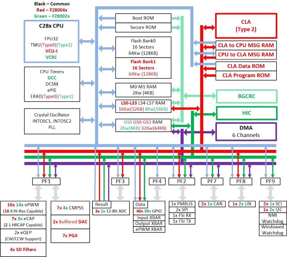
An overlaid block diagram of F28004x and F28002x is shown in Figure 1 while feature comparison of the superset part numbers for the F28002x and F28004x devices is shown in Table 1.
 Figure 1. F28002x and F28004x Overlaid Functional Block Diagram
 Table 1. F28004x and F28002x Superset Device Comparison
| Feature | F280049 F280049C | F280025 F280025C | |||||
|---|---|---|---|---|---|---|---|
| 100-Pin PZ | 64-Pin PM | 56-Pin RSH | 80-Pin PN | 64-Pin PM | 48-Pin PT | ||
| Processor and Accelerators | |||||||
| C28x | Frequency (MHz) | 100 | 100 | ||||
| FPU | Yes | Yes (with new instructions for Fast Integer Division) | |||||
| VCU-I | Yes | No | |||||
| VCRC | No | Yes | |||||
| TMU | Yes - Type 0 | Yes - Type 1 (with new instructions supporting NLPID) | |||||
| CLA – Type 2 | Available | Yes | No | ||||
| Frequency (MHz) | 100 | – | |||||
| 6-Channel DMA – Type 0 | Yes | Yes | |||||
| Memory | |||||||
| Flash | 256KB (128Kw) | 128KB (64Kw) | |||||
| RAM | Dedicated and Local Shared RAM | 36KB (18Kw) | 20KB (10Kw) | ||||
| Global Shared RAM | 64KB (32Kw) | 4KB (2Kw) | |||||
| Total RAM | 100KB (50Kw) | 24KB (12Kw) | |||||
| Code security for on-chip flash and RAM | Yes | Yes | |||||
| System | |||||||
| Configurable Logic Block (CLB) | F28004xC | F28002xC | |||||
| Motor Control Libraries in ROM | F28004xC | F28002xC | |||||
| 32-bit CPU timers | 3 | 3 | |||||
| Watchdog timers | 1 | 1 | |||||
| Nonmaskable Interrupt Watchdog (NMIWD) timers | 1 | 1 | |||||
| Crystal oscillator/External clock input | 1 | 1 | |||||
| 0-pin internal oscillator | 2 | 2 | |||||
| GPIO pins | 40 | 26 | 25 | 39 | 26 | 14 | |
| Additional GPIO | 3 (If 2-pin cJTAG is used and INTOSC used instead of X1) | 4 (If 2-pin cJTAG is used and INTOSC used instead of X1/X2) | |||||
| AIO inputs | 21 | 14 | 12 | 16 | 14 | ||
| External interrupts | 5 | 5 | |||||
| Analog Peripherals | |||||||
| ADC 12-bit | Number of ADCs | 3 | 2 | ||||
| MSPS | 3.45 | 3.45 | |||||
| Conversion Time (ns) | 300 | 300 | |||||
| ADC channels (single-ended) | 21 | 14 | 12 | 16 | 14 | ||
| Temperature sensor | 1 | 1 | |||||
| Buffered DAC | 2 | – | |||||
| CMPSS (each CMPSS has two comparators and two internal DACs) | 7 | 6 | 5 | 4 | |||
| PGA (Gain Settings: 3, 6, 12, 24) | 7 | 5 | 4 | – | |||
| Control Peripherals | |||||||
| eCAP/HRCAP modules – F28004x: Type 1 F28002x: Type 2 | 7 (2 with HRCAP capability) | 3 (1 with HRCAP capability) | |||||
| ePWM/HRPWM channels – Type 4 | 16 (16 with HRPWM capability) | 14 (8 with HRPWM capability) | |||||
| eQEP modules – F28004x: Type 1 F28002x: Type 2 | 2 | 1 | 2 | ||||
| SDFM channels – Type 1 | 4 | 3 | – | ||||
| Communication Peripherals | |||||||
| CAN – Type 0 | 2 | 1 | |||||
| I2C – Type 1 | 1 | 2 | |||||
| SCI – Type 0 | 2 | 1 | |||||
| SPI – Type 2 | 2 | 2 | |||||
| LIN – Type 1 | 1 | 2 | |||||
| PMBus – Type 0 | 1 | 1 | |||||
| FSI – Type 0 | 1 (1 RX and 1 TX) | 1 (1 RX and 1 TX) | |||||
| Package Options, Temperature, and Qualification | |||||||
| S: –40°C to 125°C (TJ) | Yes | Yes | |||||
| Q: –40°C to 125°C (TA) (AEC Q100 qualification) | Yes | No (use F280048 or F280040) | – | Yes | No (use F280024 or F280022) | Yes | |