SPRACT7 August 2020 TMS320F280021 , TMS320F280021-Q1 , TMS320F280023 , TMS320F280023-Q1 , TMS320F280023C , TMS320F280025 , TMS320F280025-Q1 , TMS320F280025C , TMS320F280025C-Q1 , TMS320F280040-Q1 , TMS320F280040C-Q1 , TMS320F280041 , TMS320F280041-Q1 , TMS320F280041C , TMS320F280041C-Q1 , TMS320F280045 , TMS320F280048-Q1 , TMS320F280048C-Q1 , TMS320F280049 , TMS320F280049-Q1 , TMS320F280049C , TMS320F280049C-Q1
2.2.1.3 Single-Shunt Current Sensing
The single-shunt current measurement technique measures the dc link current and, with knowledge of the switching states, recreates each of the three phase currents of the motor. Figure 2-7 shows the single-shunt location in the inverter circuit.
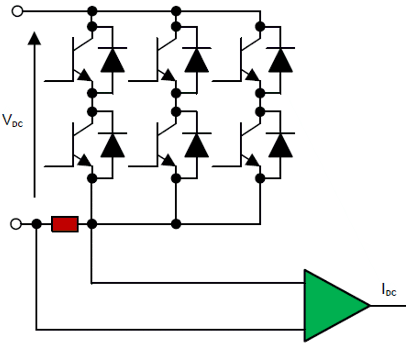 Figure 2-7 Single-Shunt Current Measurement
Circuit With Inverter
Figure 2-7 Single-Shunt Current Measurement
Circuit With InverterFor a better understanding of the measurement process and to represent the switching state of the inverter, this application note defines a switching function Sa for phase A as follows: Sa = 1 when the upper transistor of phase A is ON, and Sa = 0 when the lower transistor of phase A is ON. Similar definitions can be made for phases B and C.
The explanation of the process is based on the assumption that the inverter is fed in complementary mode. The signals in this mode, which control the lower transistors, are the opposite of Sa, Sb, Sc, which controls the upper transistors.
As previously stated, the measurement method in single-shunt current sensing depends on the switching states of the inverter switches. An example case is explained In Figure 2-8 and Figure 2-9. In Figure 2-8, the top-side switch of phase A is conducting and bottom-side switches of phase B and C are conducting. In this switching state, the DC bus current measurement gives the phase A current and is positive (+IA). The direction of current in phase A is towards the motor winding (see Figure 2-8).
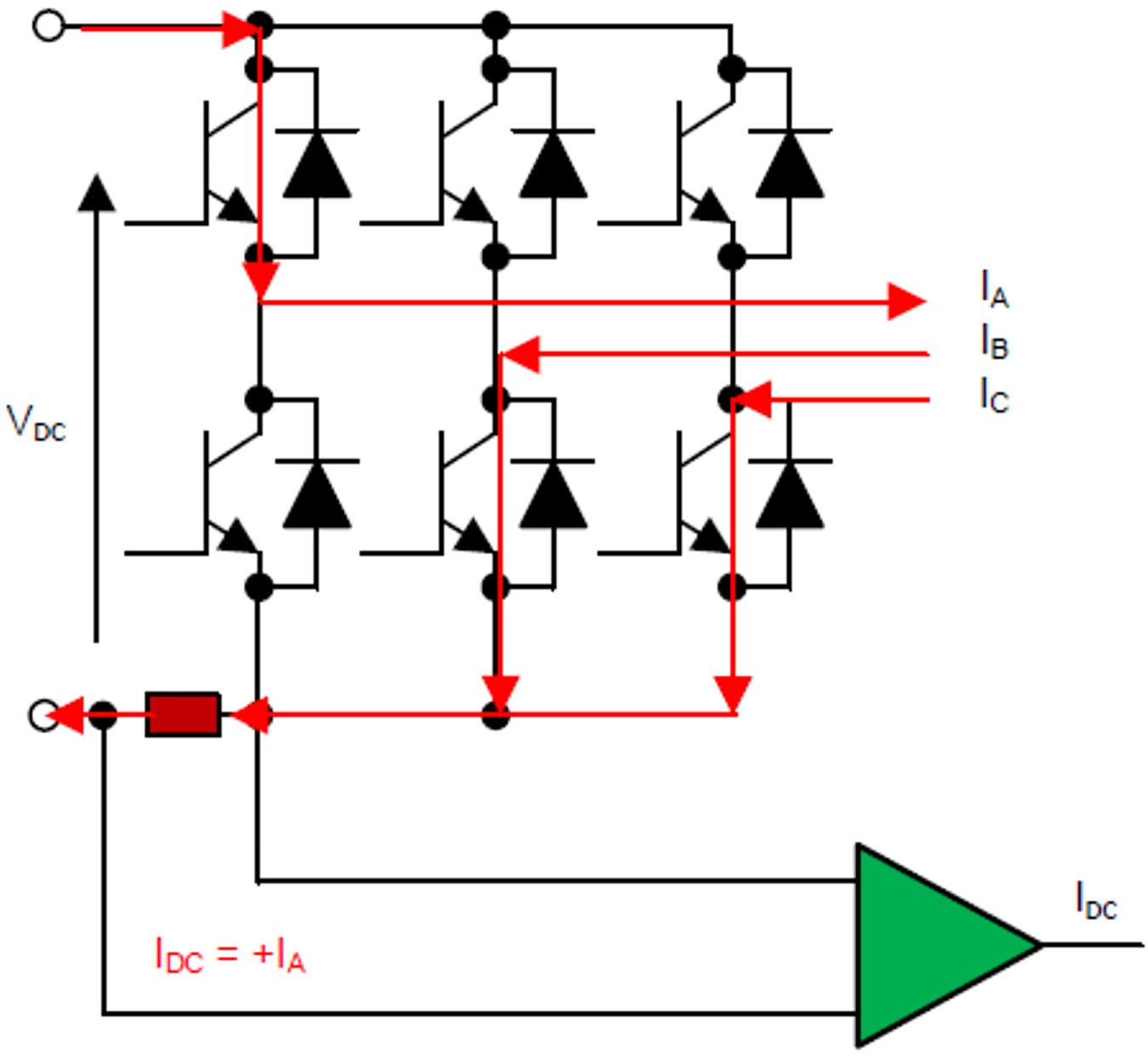 Figure 2-8 Switching Sate Sa, Sb, Sc:
100
Figure 2-8 Switching Sate Sa, Sb, Sc:
100In Figure 2-9, the top-side switches of phase A and phase B are conducting and the bottom-side switch of phase C is conducting. In this switching state, the DC bus current measurement gives the phase-C current and is negative (-IC). The direction of current in phase C is towards the inverter from the motor winding (see Figure 2-9).
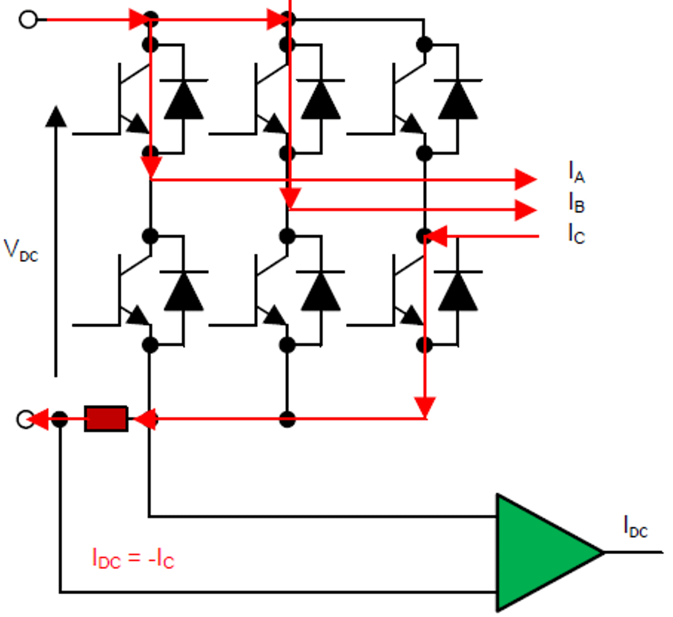 Figure 2-9 Switching Sate Sa, Sb, Sc:
110
Figure 2-9 Switching Sate Sa, Sb, Sc:
110Similar to the preceding explanation, there are eight different switch options in SVM PWM. Table 2-1 explains each one and shows the direction of the voltage space vector and what current can be measured in that state. With the switches in states 0 and 7 only circulating current is present and there is no possibility to measure current with the single-shunt technique. The six switching states from 1 to 6 are called as active vector or active voltage vector. The current measurement and switching state must both be properly considered to measure current with the single-shunt technique.
| Switch State | AH | BH | CH | Vector | Measure |
|---|---|---|---|---|---|
| 0 | 0 | 0 | 0 | • | offsets |
| 1 | 1 | 0 | 0 | → | IA |
| 2 | 1 | 1 | 0 | ↗ | -IC |
| 3 | 0 | 1 | 0 | ↖ | IB |
| 4 | 0 | 1 | 1 | ← | -IA |
| 5 | 0 | 0 | 1 | ↙ | IC |
| 6 | 1 | 0 | 1 | ↘ | -IB |
| 7 | 1 | 1 | 1 | • | offsets |
Figure 2-10 shows a SVM PWM waveform and the DC bus current measurement signal that resulted from the applied switching state. In this case the current conduction times for each switching state are on long enough so that the slew rate of the op-amp and settling time of the whole measurement system have enough time to go to steady state so that the ADC can have enough time to sample the current.
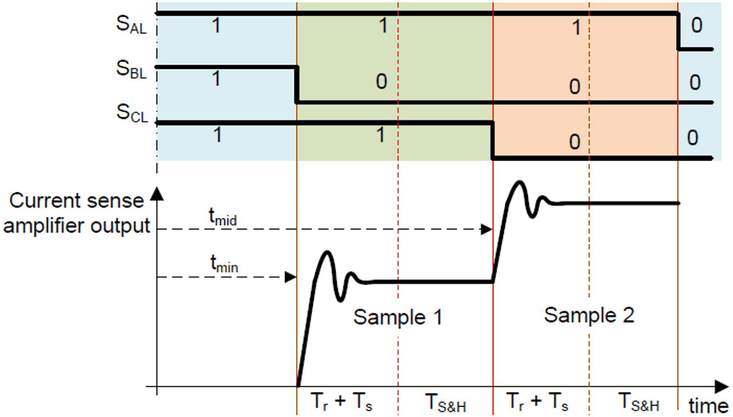 Figure 2-10 Single-Shunt Current Measurement
When Sampling Times are Sufficient
Figure 2-10 Single-Shunt Current Measurement
When Sampling Times are SufficientWhen using the single-shunt technique, it is mandatory to be able to measure current in the smallest time possible. This requirement highlights the importance of ensuring that the minimum pulse width (minimum active vector duration) and pulse transition period needs to be maintained for a valid sample. To understand the minimum vector duration required, understanding the delays in the measurement is necessary. The Figure 2-11 shows the delay components in the measurement path.
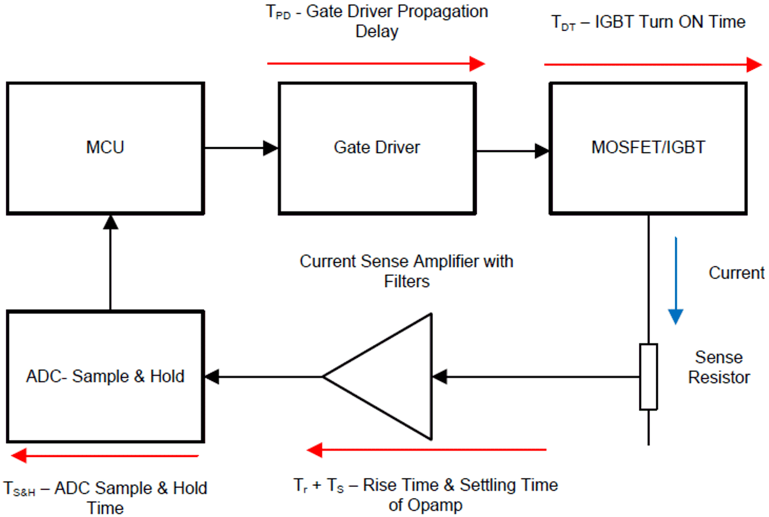 Figure 2-11 Delay in the Current Sensing
Loop
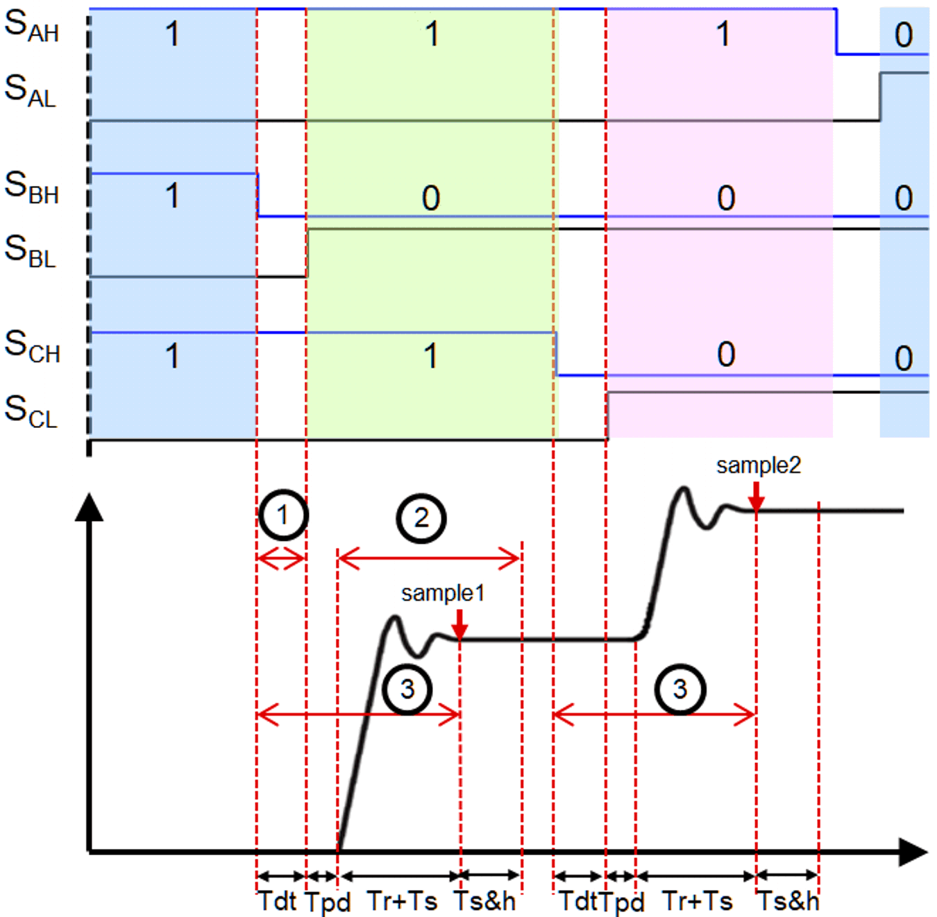 Figure 2-12 Single-Shunt Current Measurement
Timing
Figure 2-12 Single-Shunt Current Measurement
TimingThe minimum active vector duration must be more than the total delay except gate driver propagation delay in the current sensing path. The gate driver propagation delay (Tpd) only influences the calculation of sampling point. Figure 2-12 shows one of switching pattern in SVM and current wave form at the output of OpAmp. Equation 2 can be used to determine the minimum active vector duration to derive a valid current sample.
where:
- Tr = Rise time of amplifier including power switches(MOSFET/IGBT) turn on time (dependent on the amplifier slew rate and gate charging time of power switches)
- Ts = Settling time of amplifier (dependent on amplifier GBW, gain, accuracy, sensing circuit filters)
- TS&H = ADC Sample and Hold time
- TDT = Dead-time between top and bottom switch
If the duration of active vector is less than the minimum time Tmin_dur in Equation 2, it is impossible to get three-phase current from the shunt resistor.
As previously mentioned, phase currents can be sampled at zero vector state for two or three-shunt current measurement. But single-shunt currents should be sampled on each switching states of the inverter switches. So, ADC sampling point should be properly considered. From Figure 2-12, Equation 3 can be used for the sampling point calculation.
where:
- TDT = Dead-time between top and bottom switc
- TPD = Gate driver propagation delay
- Tr = Rise time of amplifier including power switches(MOSFET/IGBT) turn on time (dependent on the amplifier slew rate and gate charging time of power switches)
- Ts = Settling time of amplifier (dependent on amplifier GBW, gain, accuracy, sensing circuit filters)
Ideally, to have an undistorted current in the motor winding, the minimum active vector duration would be zero. Having the minimum active vector duration of zero is practically impossible because of the sensing and loop delay. A non-zero, minimum vector duration creates distortion in the current waveform unless it is properly compensated in the software algorithm (which is very complex and difficult to achieve). Figure 2-13 shows the space vector hexagon. As the space vector points toward the corners of the hexagon, the time window for sampling current completely disappears. There are zones located at 0°, 60°, 120°, 180°, 240°, and 300° where only one current can be measured and the other two currents must be found in another fashion. In low modulation index which is called as star area, any phase current cannot be sampled form the shunt resistor because the duration of the two active vectors applied in switching cycle are short than the minimum active duration time Tmin_dur
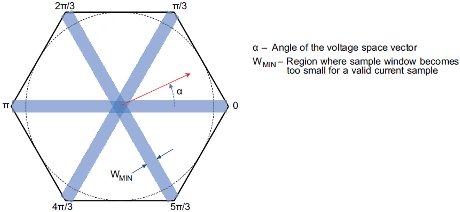 Figure 2-13 SVM and Regions Where Current
Measurement is Not Allowed
 Figure 2-14 and Figure 2-15 show the active vector durations (U1 and U2) during zero crossing and 60° sector changes. In Figure 2-14, the sector duration U1 is too small to have a valid sample. In Figure 2-15, the sector durations of U1 and U2 are too small to have a valid sample of current.
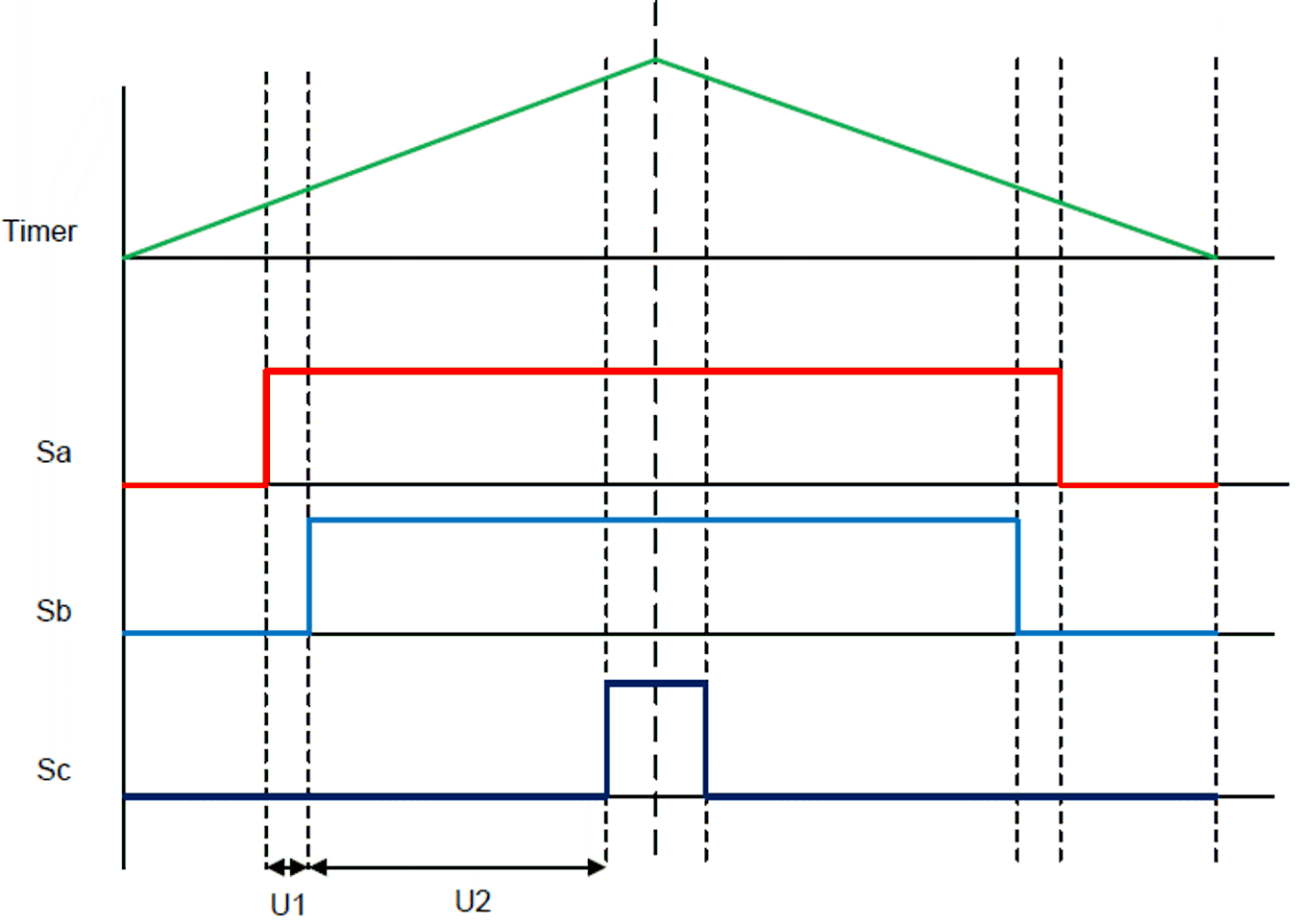 Figure 2-14 Active Vector Durations During
60° Sector Changes
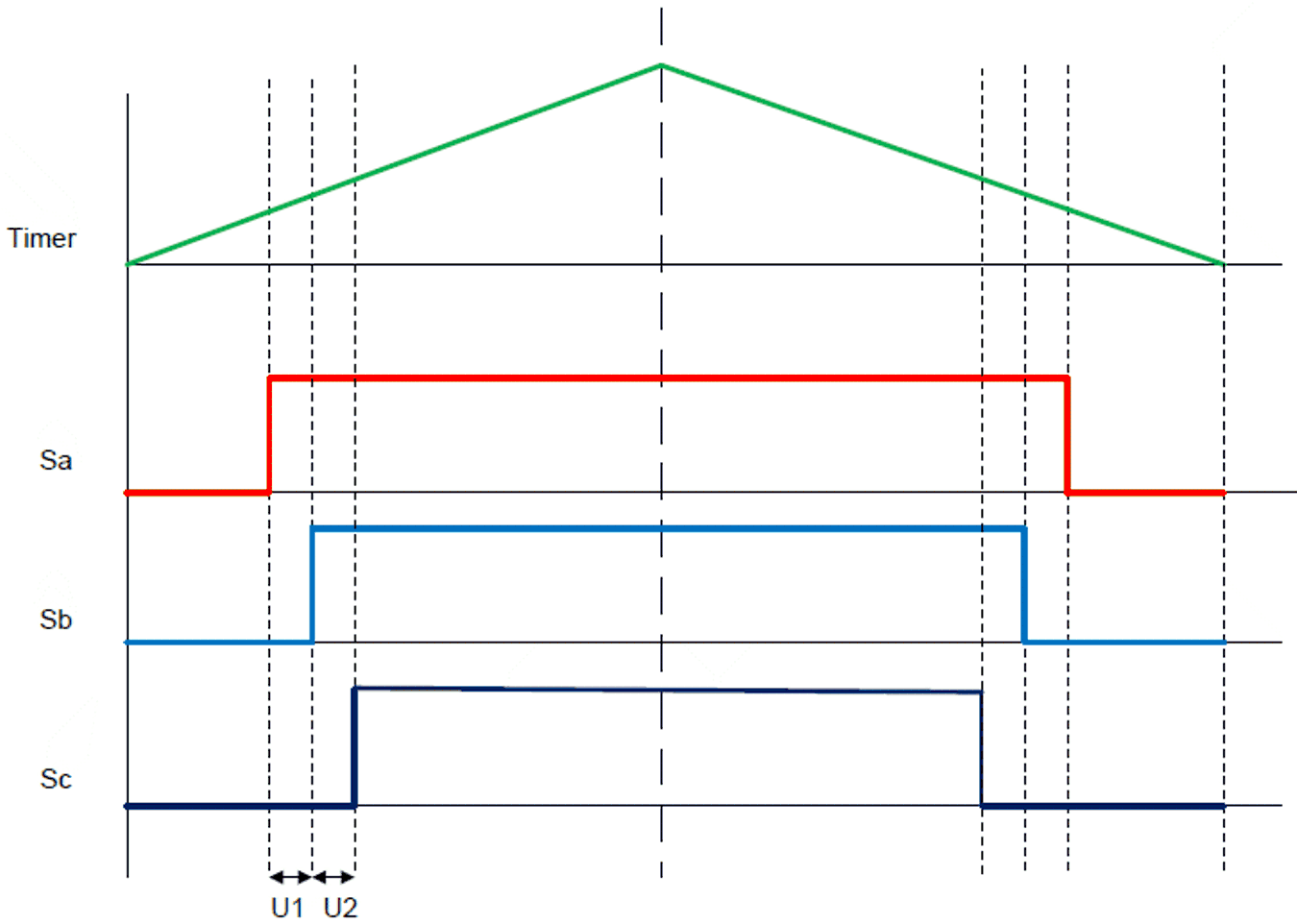 Figure 2-15 Active Vector Durations During
Zero Crossing and Low Modulation Index
Figure 2-15 Active Vector Durations During
Zero Crossing and Low Modulation IndexDesigners ideally prefer to have an accurate and fast-settling current sensing to enable the very minimum active vector duration, which offers the following advantages.
- Reduces the current sensing complexity and hence reduces actual current distortion at zero-crossing, low modulation index and sector changes (every 60° interval)
- Reduces the software overhead in determining the winding currents during the lower active vector duration; the software algorithm may use mathematical prediction or PWM phase advancing or delaying in such scenarios.
To achieve very minimum vector duration requires reducing the overall delay in the current sensing path. This task can be achieved by using a fast current sensing (using a fast amplifier with high slew rate), using a fast ADC with minimum sample & hold time, and by optimizing the dead time.