SPRACU1A October 2020 – June 2021 AM2431 , AM2432 , AM2434 , AM6411 , AM6412 , AM6421 , AM6441 , AM6442
- Trademarks
- 1Overview
-
2DDR4 Board Design and Layout Guidance
- 2.1 DDR4 Introduction
- 2.2 DDR4 Device Implementations Supported
- 2.3 DDR4 Interface Schematics
- 2.4 Compatible JEDEC DDR4 Devices
- 2.5 Placement
- 2.6 DDR4 Keepout Region
- 2.7 VPP
- 2.8 Net Classes
- 2.9 DDR4 Signal Termination
- 2.10 VREF Routing
- 2.11 VTT
- 2.12 POD Interconnect
- 2.13 CK and ADDR_CTRL Topologies and Routing Guidance
- 2.14 Data Group Topologies and Routing Guidance
- 2.15 CK and ADDR_CTRL Routing Specification
- 2.16 Data Group Routing Specification
- 2.17 Bit Swapping
-
3LPDDR4 Board Design and Layout Guidance
- 3.1 LPDDR4 Introduction
- 3.2 LPDDR4 Device Implementations Supported
- 3.3 LPDDR4 Interface Schematics
- 3.4 Compatible JEDEC LPDDR4 Devices
- 3.5 Placement
- 3.6 LPDDR4 Keepout Region
- 3.7 Net Classes
- 3.8 LPDDR4 Signal Termination
- 3.9 LPDDR4 VREF Routing
- 3.10 LPDDR4 VTT
- 3.11 CK and ADDR_CTRL Topologies
- 3.12 Data Group Topologies
- 3.13 CK and ADDR_CTRL Routing Specification
- 3.14 Data Group Routing Specification
- 3.15 Channel, Byte, and Bit Swapping
- 4Revision History
2.3.1 DDR4 Implementation Using 16-Bit SDRAM Devices
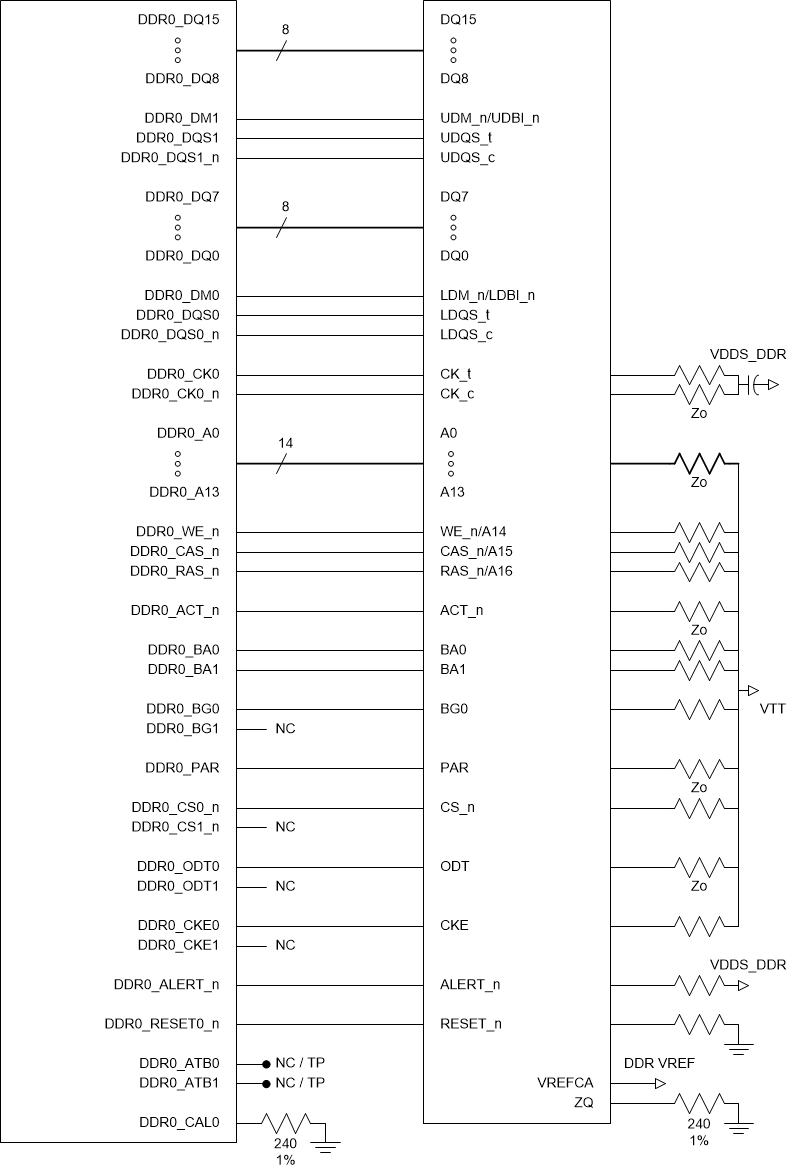
The DDR4 interface schematics vary, depending upon the width of the DDR4 SDRAM devices used and the width of the EMIF bus implemented. General connectivity is straightforward and consistent between the implementations. 16-bit SDRAM devices look like two 8-bit devices. Figure 2-1 shows the schematic connections for a 16-bit interface using a single x16 SDRAM.
When not using one of the byte lanes on the processor, the proper method of handling the unused pins is to tie off the unused DDR_DQSxP pins to ground through a 1k-Ω resistor and to tie off the unused DDR_DQSxN pins to the VDDS_DDR supply, also referred to as the I/O supply VDDQ, through a 1k-Ω resistor. This must be done for each byte not used. Although these signals have internal pullups and pulldowns, external pullups and pulldowns provide additional protection against external electrical noise causing activity on the signals.
 Figure 2-1 16-Bit, Single-Rank DDR4
Implementation Using x16 SDRAM