SPRACY2 May 2021 TMUX646
2 PCB Design Guidelines
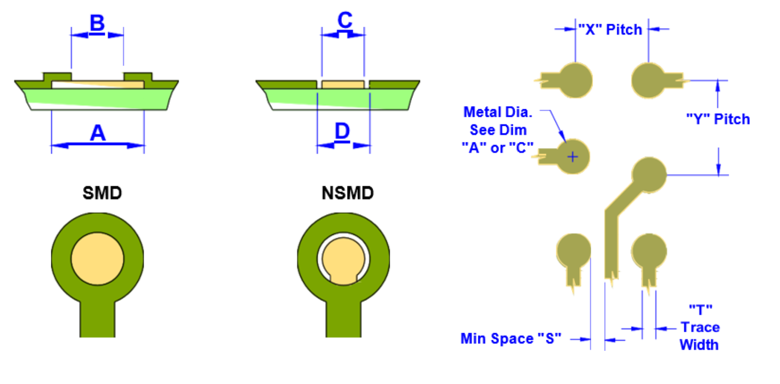
The PCB design guidelines outlined in the Conductor Width/Spacing section of nFBGA Packaging are still applicable to small body nFBGAs. Figure 2-1, Table 2-1 and Table 2-2 outline examples of specific pad, trace, and width dimensions for small body packages.
 Figure 2-1 Solder Pad and Trace
Dimensions
Figure 2-1 Solder Pad and Trace
DimensionsTable 2-1 Sample Small Body nFBGA Solder Pad
Details
| Solder Mask Defined Pad (SMD) | Non-Solder Mask Defined Pad (SMD) | |||
|---|---|---|---|---|
| Package Designator | Copper Pad (A) | Solder Mask Opening (B) | Copper Pad (C) | Solder Mask Opening (D) |
| ZWA | 0.35 mm | 0.25 mm | 0.25 mm | 0.35 mm |
| ZEC | 0.30 mm | 0.23 mm | 0.23 mm | 0.30 mm |
Table 2-2 Trace Width Spacing
Examples
| Pitch (mm) | Metal Diameter (“A” or ”C”) | Trace Width/ Spacing (“S” or “T”) |
|
|---|---|---|---|
| SMD pad | 0.40 | 0.35 | 0.05 |
| 0.50 | 0.10 | ||
| NSMD Pad | 0.40 | 0.25 | 0.08 |
| 0.50 | 0.13 |
TI recommends the use of type 3 or finer solder paste when mounting nFBGA. The use of paste offers the following advantages:
- It acts as a flux to aid wetting of the solder ball to the PCB land.
- The adhesive properties of the paste will hold the component in place during reflow.
- Paste contributes to the final volume of solder in the joint, and thus allows this volume to be varied to give an optimum joint.
- Paste selection is normally driven by overall system assembly requirements. In general, the "noclean" compositions are preferred due to the difficulty in cleaning under the mounted components.
TI recommends a pressure safety zone in mounting the nFBGA package. Recommended force should be controlled to 5N maximum for static and 2.5N for impact.