SPRAD59 October 2023 TMS320F280039
5 Message RAM Configuration
In DCAN, Message RAM can only be accessed by the Message Handler. The Driverlib APIs interact with the Message Interface (IFx) registers which carry out the read or write operations with the Message RAM. In MCAN, Driverlib APIs can be used to carry out the read or write operations with the Message RAM directly.
The Message RAM is structured differently in MCAN as compared to DCAN. In DCAN, the number of message objects in the Message RAM is fixed at 32 and each message object can be configured for either transmit or receive operation.
However, in MCAN, Message RAM can be configured to have the following sections:
- Standard Filter Element
- Extended Filter Element
- Rx Buffer
- Rx FIFO
- Tx Buffer
- Tx FIFO or Tx Queue
- Tx Event FIFO
The design of MCAN Message RAM offers tremendous flexibility, enabling allocation of the available memory to each of the sections mentioned above based on the application needs. The sections can be ordered in any manner and the unused sections can be allocated zero memory. Note that Message RAM size can vary from one device to another. Refer the device-specific data sheet for more information.
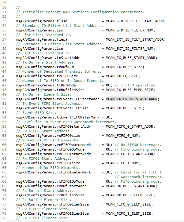
Message RAM configuration involves defining the following:
- Starting address for every section used.
- The number of elements in each section.
- The size of the elements which is different for different size of data packets as can be seen in Table 5-1 (Filter Elements and Tx Event FIFO have fixed sizes).
These values are written to specific registers and are subsequently used by both the Message Handler and Driverlib APIs to interact with the Message RAM. Hence, Message RAM configuration is a crucial step for MCAN during module initialization, while such configuration is not required in DCAN. The MCAN module addresses the Message RAM in 32-bit words. Consequently, all sections are of sizes that are multiples of 32-bit words.
| MCAN_RXESC.RBDS/ MCAN_RXESC.F0DS/ MCAN_RXESC.F1DS/ MCAN_TXESC.TBDS (Corresponding to Rx Buffer, Rx FIFOs and Tx Buffer, respectively) |
Data Field (bytes) | FIFO Element Size (or) Buffer Element Size [RAM words] |
|---|---|---|
| 000 | 8 | 4 |
| 001 | 12 | 5 |
| 010 | 16 | 6 |
| 011 | 20 | 7 |
| 100 | 24 | 8 |
| 101 | 32 | 10 |
| 110 | 48 | 14 |
| 111 | 64 | 18 |
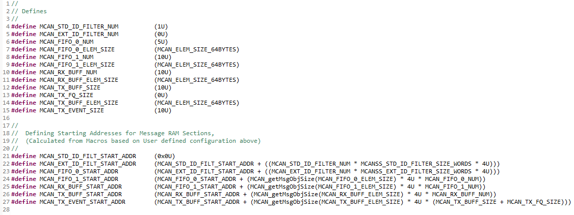
Macros are available in C2000ware examples which automatically calculate the starting address for each section when the number and size of elements are set by the user. This configuration can be successfully utilized in any application. Multiple valid configurations are possible and there is not a single "correct" configuration. Note that the MCAN module does not check for invalid configurations. It is the responsibility of the user to verify that sections do not overlap each other or exceed the available RAM.
 Figure 5-1 MCAN
Message RAM Macros
 Figure 5-2 MCAN
Message RAM Initialization