SPRAD61A March 2023 – November 2023 AM2732 , AM2732 , AM2732-Q1 , AM2732-Q1
- 1
- Abstract
- Trademarks
- 1 Introduction
- 2 Power
- 3 Clocking
- 4 Resets
- 5 Bootstrapping
- 6 JTAG Emulators and Trace
- 7 Multiplexed Peripherals
- 8 Digital Peripherals
- 9 Layer Stackup
- 10Vias
- 11BGA Power Fan-Out and Decoupling Placement
- 12References
- 13Revision History
5.2 QSPI Memory Controller Implementation
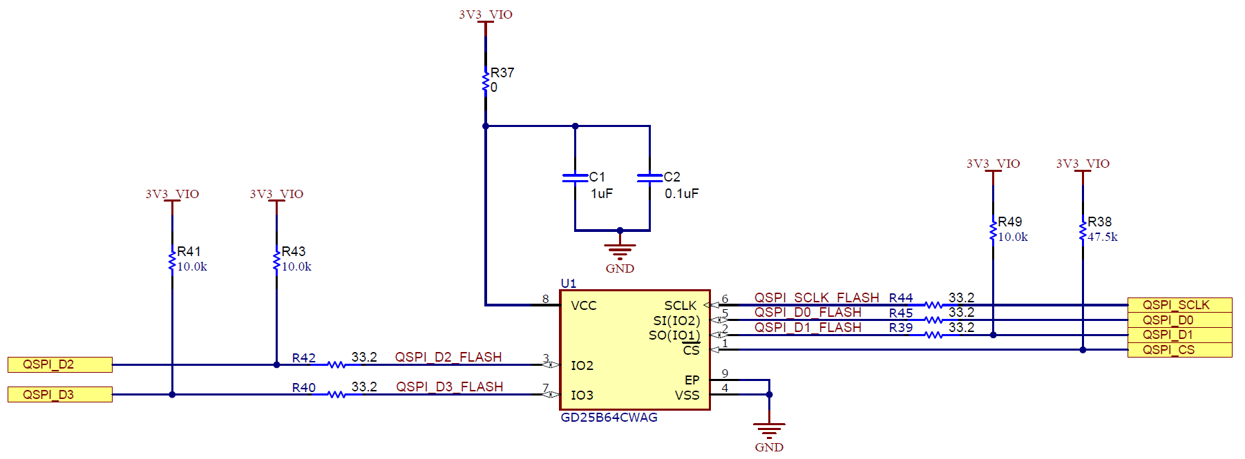
The QSPI memory is the primary boot memory location for the AM273x MCU. Good signal integrity of this memory interface is critical for basic QSPI boot operations of the AM273x MCU. Additional pull-up resistors are also necessary.
- Include a chip-select pull-up resistor to ensure that the device is normally read/write disabled until the AM273x QSPI controller drives chip-select low at the start of a new read/write transaction.
- Include a pull resistor to disable write protect mode by default
- Include a pull resistor to disable hold mode by default
 Figure 5-2 Excerpt From AM273x GPEVM Schematic – AM273x QSPI Controller and GD25B64CWAG NOR Flash Memory
Additional routing guidelines for the QSPI memory interface are provided in Figure 5-3 and Table 5-2 These should be used as maximum routing and skew match limits.
 Figure 5-3 AM273x QSPI - Routing Rules Diagram
| Spec No. | Specification | Value | Unit |
|---|---|---|---|
| 1 | QSPI_CLK, QSPI_CS0, QSPI_D[3:0] maximum delay | 450 | ps |
| 2 | QSPI_CLK to QSPI_D[3:0] maximum skew | 50 | ps |
| 3 | Approximate maximum routing distances | 3214 | mils |
| 4 | Approximate maximum routing skew | 357 | mils |
| 5 | A series termination resistor (R1 in diagram above) should be placed close to the QSPI_CLK transmit pin of the AM273x to control rise-time and reflections of the clock line. | Variable, 0 to 40 | Ω |
| 6 | A series termination resistor (R2 in diagram above) should be placed close to the QSPI data pins of the attached memory to control rise-time and reflections of the data lines. | Variable, 0 to 40 | Ω |
It is recommended that the QSPI memory be co-located close to the AM273x BGA footprint, which allows for routing that maximizes the delay margins and skew margins. As seen in Figure 5-3 it is also recommended to include a series termination resistor near the QSPI controller clock transmit pin. Similarly, series terminations should be added at the data pins of the QSPI device as well. During read quad-read operations, which will be the most used mode of operation of the memory, this helps create well controlled edges on the data lines.