SPRAD61A March 2023 – November 2023 AM2732 , AM2732 , AM2732-Q1 , AM2732-Q1
- 1
- Abstract
- Trademarks
- 1 Introduction
- 2 Power
- 3 Clocking
- 4 Resets
- 5 Bootstrapping
- 6 JTAG Emulators and Trace
- 7 Multiplexed Peripherals
- 8 Digital Peripherals
- 9 Layer Stackup
- 10Vias
- 11BGA Power Fan-Out and Decoupling Placement
- 12References
- 13Revision History
11.3.1.2 3.3V Digital and Analog Layout - ZCE Four Layer Example
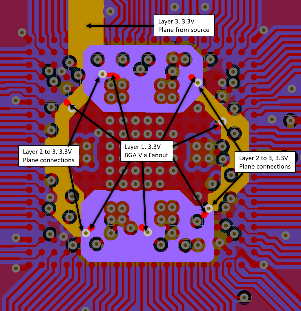
On the AM273 NZN Four Layer Example, the 3.3 V plane is shown routing to and underneath the AM273 device primarily on layer 3. Due to routing limitations caused by a four layer PCB, underneath the AM273 device the 3.3 V plane is split between layer 2 and layer 3.
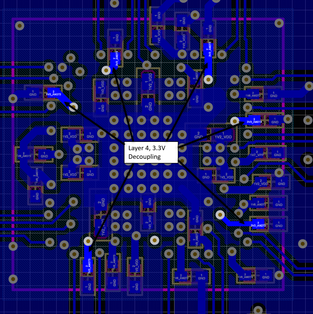
The 3.3 V planes on layer 2 break up the otherwise solid ground pour on layer 2. The placement of these cutouts was chosen to minimize the impact to the signal return paths for as many GPIO pins as possible. Vias connect the planes on layers 2 and 3 to the BGA ball pads on the top layer and the decoupling capacitors on the bottom layer.
 Figure 11-17 ZCE
4 Layer Example Excerpt – 3.3 V Digital and Analog
Power Planes on Layers 2 and 3 and BGA Vias
  Figure 11-18 ZCE
4 Layer Example Excerpt – 3.3 V Decoupling