SPRAD61A March   2023  – November 2023 AM2732 , AM2732 , AM2732-Q1 , AM2732-Q1


  1.   1
  2.   Abstract
  3.   Trademarks
  4. Introduction
    1. 1.1 Acronyms
  5. Power
    1. 2.1 Discrete DC-DC Power Solution
    2. 2.2 Integrated PMIC Power Solution
    3. 2.3 Power Decoupling and Filtering
    4. 2.4 Power Consumption
  6. Clocking
    1. 3.1 Crystal and Oscillator Input Options
    2. 3.2 Output Clock Generation
    3. 3.3 Crystal Selection and Shunt Capacitance
    4. 3.4 Crystal Placement and Routing
  7. Resets
  8. Bootstrapping
    1. 5.1 SOP Signal Implementation
    2. 5.2 QSPI Memory Controller Implementation
    3. 5.3 ROM QSPI Boot Requirements
  9. JTAG Emulators and Trace
  10. Multiplexed Peripherals
  11. Digital Peripherals
    1. 8.1 General Digital Peripheral Routing Guidelines
  12. Layer Stackup
    1. 9.1 TMDS273GPEVM Layer Stackup
      1. 9.1.1 TMDS273GPEVM Key Stackup Features
    2. 9.2 Four Layer ZCE Example Layer Stackup
      1. 9.2.1 ZCE Four Layer Example Key Stackup Features
    3. 9.3 Four Layer NZN Example Layer Stackup
      1. 9.3.1 NZN Four Layer Example Key Stackup Features
  13. 10Vias
  14. 11BGA Power Fan-Out and Decoupling Placement
    1. 11.1 Ground Return
      1. 11.1.1 Ground Return - TMDS273GPEVM
      2. 11.1.2 Ground Return - ZCE Four Layer Example
      3. 11.1.3 Ground Return - NZN Four Layer Example
    2. 11.2 1.2 V Core Digital Power
      1. 11.2.1 1.2 V Core Digital Power Key Layout Considerations
        1. 11.2.1.1 1.2V Core Layout - TMDS273GPEVM
        2. 11.2.1.2 1.2V Core Layout - ZCE Four Layer Example
        3. 11.2.1.3 1.2V Core Layout - NZN Four Layer Example
    3. 11.3 3.3 V Digital and Analog Power
      1. 11.3.1 3.3 V Digital and Analog Power Key Layout Considerations
        1. 11.3.1.1 3.3V Digital and Analog Layout - TMDS273GPEVM
        2. 11.3.1.2 3.3V Digital and Analog Layout - ZCE Four Layer Example
        3. 11.3.1.3 3.3V Digital and Analog Layout - NZN Four Layer Example
    4. 11.4 1.8 V Digital and Analog Power
      1. 11.4.1 1.8 V Digital and Analog Power Key Layout Considerations
        1. 11.4.1.1 1.8V Digital and Analog Layout - TMDS273GPEVM
        2. 11.4.1.2 1.8V Digital and Analog Layout - ZCE Four Layer Example
        3. 11.4.1.3 1.8V Digital and Analog Layout - NZN Four Layer Example
  15. 12References
  16. 13Revision History

Crystal Placement and Routing

Crystal oscillator input should be placed as close as possible to the AM273x CLKM/P pads with minimal length traces between crystal and AM273x pads. A ground ring shorted to the local VSS plane should be placed adjacent and between the CLKM and CLKP traces to help prevent coupling from adjacent signals onto the clock higher impedance crystal input paths.
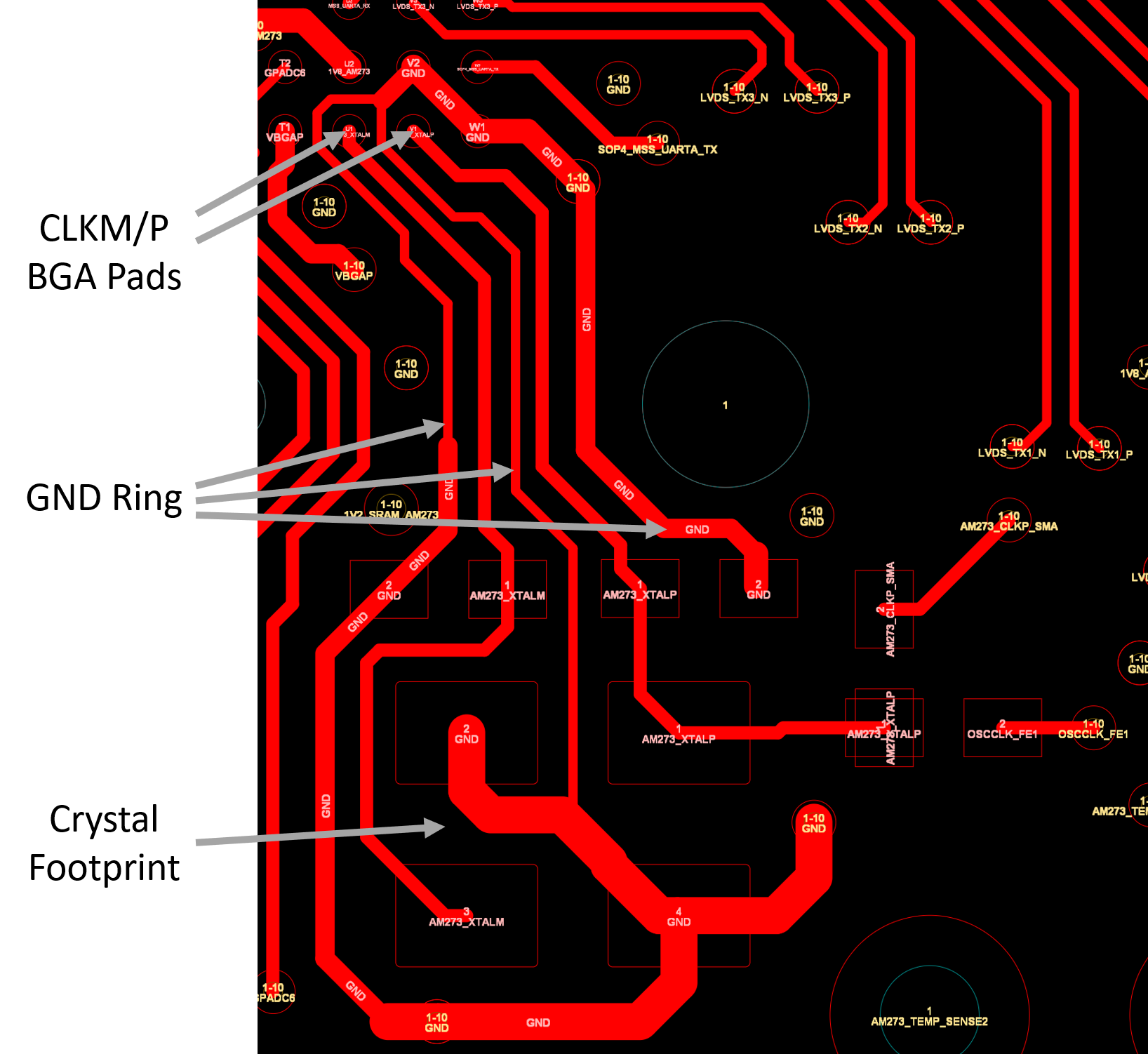
GUID-04561331-7B4A-4679-B6CD-0A832A549640-low.png Figure 3-2 Excerpt From AM273x GPEVM Layout - Crystal Layout and Ground Ring Structure