SPRAD62 February 2023 F29H850TU , TMS320F280023C , TMS320F280025C , TMS320F280025C-Q1 , TMS320F280037C , TMS320F280037C-Q1 , TMS320F280038C-Q1 , TMS320F280039C , TMS320F280039C-Q1 , TMS320F28386D , TMS320F28386D-Q1 , TMS320F28386S , TMS320F28386S-Q1 , TMS320F28388D , TMS320F28388S , TMS320F28P650DH , TMS320F28P650DK , TMS320F28P650SH , TMS320F28P650SK , TMS320F28P659DH-Q1 , TMS320F28P659DK-Q1 , TMS320F28P659SH-Q1
- Abstract
- Trademarks
- 1Introduction
- 2Serial Port Design Methodology
- 3Example A: Using the CLB to Input and Output a TDM Stream in Audio Applications
- 4Example B: Using the CLB to Implement a Custom Communication Bus for LED Driver in Lighting Applications
- 5References
3.6 Step 5: Simulate the Logic Design
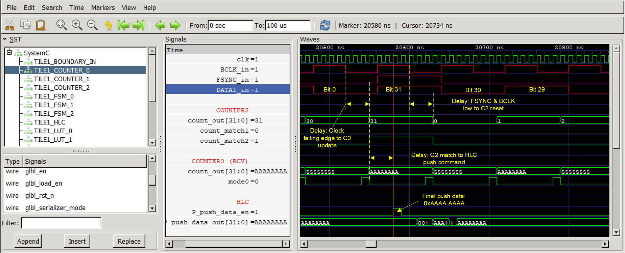
A data receive operation is simulated in Figure 3-9. For this simulation a simple pattern of 0xAAAA AAAA is used as data input. The simulation shows the transition between the last bit of the last word in the TDM frame and the start of a new frame.
 Figure 3-9 TDM-8 Data Receive
Simulation
Figure 3-9 TDM-8 Data Receive
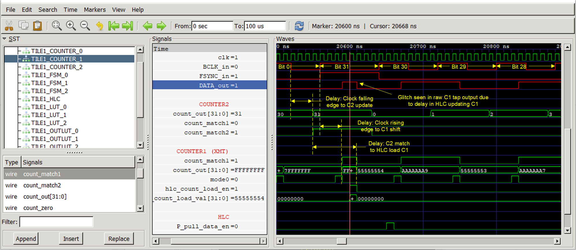
SimulationA data transmit operation is simulated in Figure 3-10. The simulation shows the transition between the last bit of the last word in the TDM frame and the start of a new frame. For this simulation a pattern of 0x5555 5554 is continuously transmitted to highlight the potential for a brief glitch at the output of the serializer in between serial words. Since the serializer must be loaded after it has shifted its counter value to avoid losing the most significant bit in the transmit word, there is a brief period of time when the serializer output is invalid.
 Figure 3-10 TDM-8 Data Transmit
Simulation
Figure 3-10 TDM-8 Data Transmit
SimulationNotice that in this TDM example the HLC has been configured to push the value in C0 to the FIFO and then load a new value to C1 (see Figure 3-5). This is done deliberately to ensure C1 is loaded after the rising edge of BCLK_IN. Since the HLC action is triggered on the falling edge of BCLK and the serializer action is dependent on the rising edge of BCLK, there is an inherent dependency on the BCLK_IN period. If the BCLK_IN period is extended (BCLK_IN frequency is reduced or CLB clock frequency is increased), there is a risk that the C1 update happens before the rising edge of the clock, which causes a loss of the most-significant bit in the serial word.
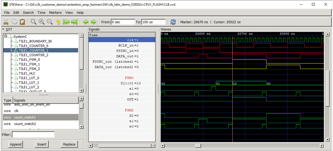
As seen in Figure 3-10, there is a delay between the output data and the input FSYNC and BCLK. In order to output a FSYNC and DATA1 signal that are synchronized with each other, two FSMs are used to latch and delay these two signals. The simulation result of this feature is shown in Figure 3-11.
 Figure 3-11 FSYNC and DATA1
Synchronization