SPRAD66A February 2023 – December 2023 AM62A3 , AM62A3-Q1 , AM62A7 , AM62A7-Q1 , AM62P , AM62P-Q1
- 1
- AM62Ax/AM62Px LPDDR4 Board Design and Layout Guidelines
- Trademarks
- 1Overview
-
2LPDDR4 Board Design and Layout Guidance
- 2.1 LPDDR4 Introduction
- 2.2 LPDDR4 Device Implementations Supported
- 2.3 LPDDR4 Interface Schematics
- 2.4 Compatible JEDEC LPDDR4 Devices
- 2.5 Placement
- 2.6 LPDDR4 Keepout Region
- 2.7 Net Classes
- 2.8 LPDDR4 Signal Termination
- 2.9 LPDDR4 VREF Routing
- 2.10 LPDDR4 VTT
- 2.11 CK and ADDR_CTRL Topologies
- 2.12 Data Group Topologies
- 2.13 CK0 and ADDR_CTRL Routing Specification
- 2.14 Data Group Routing Specification
- 2.15 Channel, Byte, and Bit Swapping
- 2.16 Data Bus Inversion
- 3LPDDR4 Board Design Simulations
- 4Appendix: SOC Package Delays
- 5References
- 6Revision History
3.4 Time Domain Reflectometry (TDR) Analysis
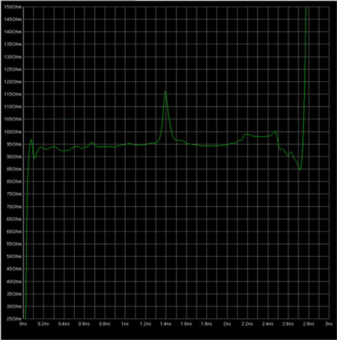
As a lot of the design fixes are targeted towards maintaining uniform trace impedance, an important analysis method used in assessing the quality of the design is the Time Domain Reflectometry (TDR) analysis. This plots the impedance of a trace as a function of its length, as shown in Figure 3-1.
 Figure 3-1 TDR Plot Example With Impedance Mismatch
As shown in Figure 3-1, the TDR plot highlights impedance discontinuities in the trace from one end to the other. This method depends on a reflected waveform from the far-end of the trace. The delay in the plot corresponding to a particular point in the trace actually corresponds to 2 times the distance of that point from the source, owing to the round trip time. This needs to be factored in for assessing the source of impedance discontinuities.
The TDR plot can be generated by reading in the S-parameter models generated by the extraction tool and assessing them in “Time-Domain” mode. A standard EDA simulator such as HyperLynx can perform this function. It is recommended to optimize the design to within a ± 5% deviation from the nominal trace impedance.
The TDR plots are not pass/fail tests, but rather is more of a guide to check if the design has a reasonable chance of performing a the required level.