SPRAD66B February 2023 – December 2024 AM62A3 , AM62A3-Q1 , AM62A7 , AM62A7-Q1 , AM62D-Q1 , AM62P , AM62P-Q1
- 1
- AM62Ax, AM62Px, AM62Dx LPDDR4 Board Design and Layout Guidelines
- Trademarks
- 1Overview
-
2LPDDR4 Board Design and Layout Guidance
- 2.1 LPDDR4 Introduction
- 2.2 LPDDR4 Device Implementations Supported
- 2.3 LPDDR4 Interface Schematics
- 2.4 Compatible JEDEC LPDDR4 Devices
- 2.5 Placement
- 2.6 LPDDR4 Keepout Region
- 2.7 Net Classes
- 2.8 LPDDR4 Signal Termination
- 2.9 LPDDR4 VREF Routing
- 2.10 LPDDR4 VTT
- 2.11 CK and ADDR_CTRL Topologies
- 2.12 Data Group Topologies
- 2.13 CK0 and ADDR_CTRL Routing Specification
- 2.14 Data Group Routing Specification
- 2.15 Channel, Byte, and Bit Swapping
- 2.16 Data Bus Inversion
- 3LPDDR4 Board Design Simulations
- 4Additional Information: SOC Package Delays
- 5Summary
- 6References
- 7Revision History
3.5.1 Simulation Setup
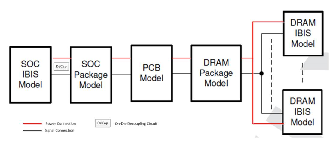
Set up the system-level schematic in the simulator by connecting the SOC IBIS model, board model, power supplies, DRAM package model, and DRAM IBIS model. A typical system-level DDR schematic is shown in Figure 3-2.
Note: Be cautious of the DRAM
configuration (number of dies in the package, number of ranks, and
number of channels) while setting up the system schematic. Be
cautious that the DRAM configuration can also include on-die
decoupling circuit.
 Figure 3-2 Typical
System-Level DDR Schematic
Figure 3-2 Typical
System-Level DDR Schematic- LPDDR4 simulations require power-aware IBIS models for the controller and the memory along with a simulator that supports channel simulations for DDR interfaces.
- SPICE-based transistor-level simulations cannot be used for generating BER signal eyes. Use a simulator that can handle power-aware IBIS simulations and can run channel simulations for the DDR interface.
- IBIS models reduce simulation time with minimal loss in accuracy compared with SPICE-based transistor-level simulations. IBIS models starting from version 5.0 are power-aware models which enables Simultaneous Switching Output (SSO) noise simulations. The TI IBIS model is a power-aware IBIS model.
- Use SPICE models to accurately model the on-die decoupling capacitance on the DDR supply net for both controller and DRAM. This makes sure of accurate power noise and Power Supply Induced Jitter (PSIJ) estimation in DDR simulations. The on-die decoupling capacitance information for the DRAM can be obtained from the DRAM vendor.
- Use SPICE or S-parameter files to model the DRAM package. This can be requested from the DRAM vendor. EBD models are not recommended.
- Note that inside the SoC IBIS model, there is a section for the package that contains an RLC matrix for all signal and power nets including DDR. TI recommends to use the SoC IBIS model, not the SOC package S-parameter model. When using SoC IBIS model, make sure to check the Package Parasitics (or equivalent parameter in the simulation tools) and use the Package Model model type which contains fully coupled L/C information on a per pin basis (denoted in the IBIS file as [Package Model] am62_pkg).
- AM62Ax,
AM62Px, AM62Dx model for
the on-die decoupling capacitance on the DDR supply net:
- Data
****************************************** * On-die Decoupling circuit for AM62Ax, AM62Px, AM62Dx (DIE_VDDS_DDR to VSS) ****************************************** * Notes: * Includes on-die decoupling for all DDR signals * * This subcircuit must be added across the AM62Ax, AM62Px, AM62Dx IBIS model's * DIE_VDDS_DDR and VSS pins * ****************************************** * x_decouple DIE_VDDS_DDR vss_die AM62Ax, AM62Px, AM62Dx_ondie_decoupling_alldq ****************************************** .SUBCKTAM62Ax, AM62Px, AM62Dx_ondie_decoupling_alldq DIE_VDDS_DDR vss_die Cvddq_c DIE_VDDS_DDR DIE_VDDS_DDR_c 1.324741e-9 Rvddq_c vss_die DIE_VDDS_DDR_c 25.0036612e-3 .ENDS - Address/Command
******************************************
* On-die Decoupling circuit for AM62Ax,
                    AM62Px, AM62Dx (DIE_VDDS_DDR to VSS)
******************************************
* Notes:
* Includes on-die decoupling for all DDR signals
*
* This subcircuit must be added across the AM62Ax,
                    AM62Px, AM62Dx IBIS model's
* DIE_VDDS_DDR and VSS pins
*
******************************************
* x_decouple DIE_VDDS_DDR vss_die AM62Ax,
                    AM62Px, AM62Dx_ondie_decoupling_alldq
******************************************
.SUBCKTAM62Ax,
                    AM62Px, AM62Dx_ondie_decoupling_alldq DIE_VDDS_DDR vss_die
Cvddq_c  DIE_VDDS_DDR DIE_VDDS_DDR_c 4.335517e-9
Rvddq_c  vss_die DIE_VDDS_DDR_c 25.0036612e-3
.ENDS
- Data