SPRAD66B February 2023 – December 2024 AM62A3 , AM62A3-Q1 , AM62A7 , AM62A7-Q1 , AM62D-Q1 , AM62P , AM62P-Q1
- 1
- AM62Ax, AM62Px, AM62Dx LPDDR4 Board Design and Layout Guidelines
- Trademarks
- 1Overview
-
2LPDDR4 Board Design and Layout Guidance
- 2.1 LPDDR4 Introduction
- 2.2 LPDDR4 Device Implementations Supported
- 2.3 LPDDR4 Interface Schematics
- 2.4 Compatible JEDEC LPDDR4 Devices
- 2.5 Placement
- 2.6 LPDDR4 Keepout Region
- 2.7 Net Classes
- 2.8 LPDDR4 Signal Termination
- 2.9 LPDDR4 VREF Routing
- 2.10 LPDDR4 VTT
- 2.11 CK and ADDR_CTRL Topologies
- 2.12 Data Group Topologies
- 2.13 CK0 and ADDR_CTRL Routing Specification
- 2.14 Data Group Routing Specification
- 2.15 Channel, Byte, and Bit Swapping
- 2.16 Data Bus Inversion
- 3LPDDR4 Board Design Simulations
- 4Additional Information: SOC Package Delays
- 5Summary
- 6References
- 7Revision History
3.5.3.3 Mask Report
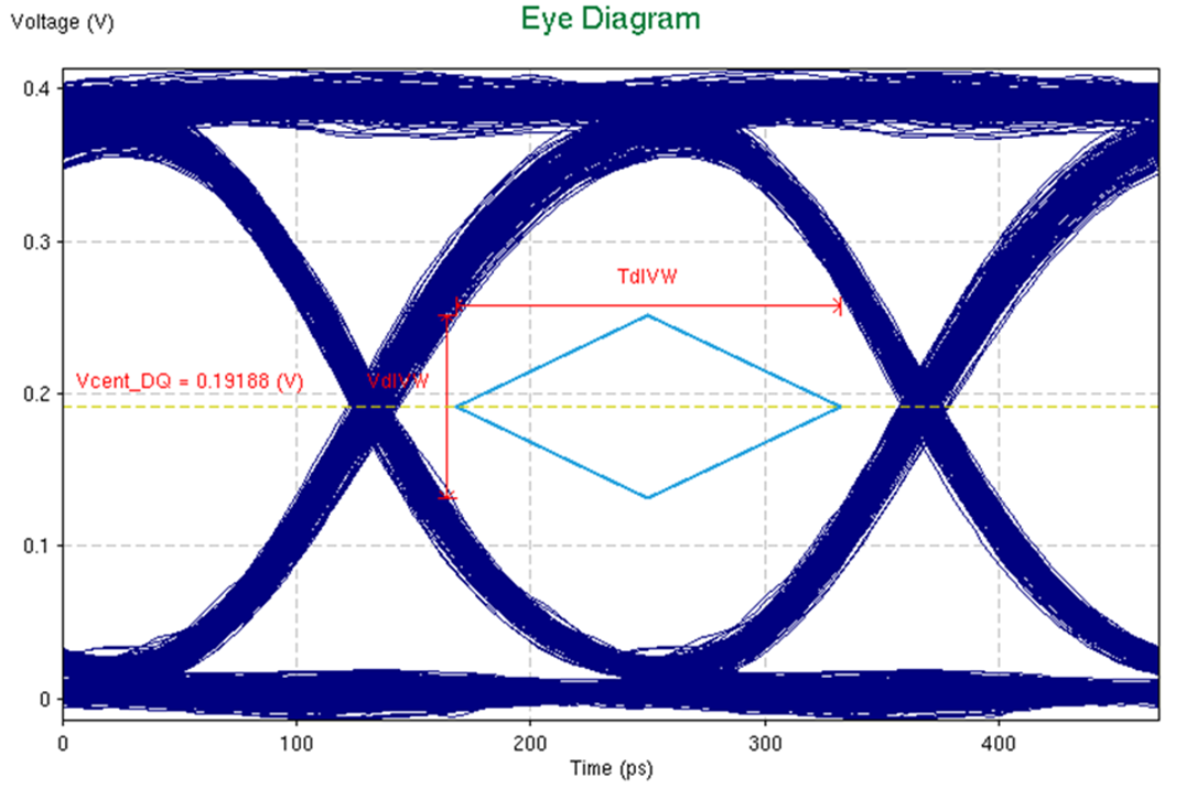
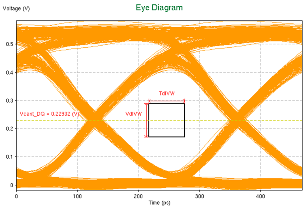
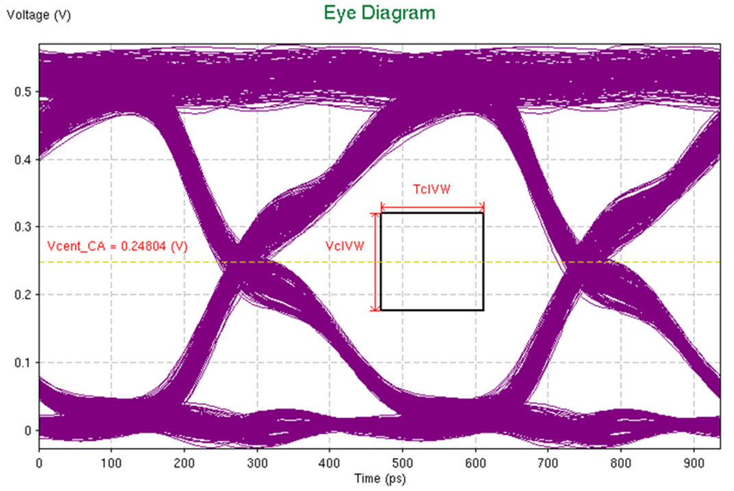
The minimum jitter and noise margins are to be captured with respect to the eye masks. This masks are data rate dependent, and includes:
- Data read eye mask at the SOC die pad for functionality testing.
- Data write eye mask (JEDEC spec) at the DRAM pin/BGA for compliance testing.
- CA bus eye mask (JEDEC spec) at the DRAM pin/BGA for compliance testing.
There is at least two sets of eye diagrams generated by the simulator:
- Vref set to the best Vref of the byte offset by the Vref_set_tol in the positive direction (Vref_set_tol is defined in JEDEC spec).
- Vref set to the best Vref of the byte offset by the Vref_set_tol in the negative direction.
The system-level margins are the worst case noise and jitter margins from all eye diagram measurements listed above (across SSHT and FFLT corners). For all waveforms captured at the DRAM device, margins must be calculated at both the BGA pin and the DRAM pad.
| Parameter | Mask Shape | LPDDR4-1600 | LPDDR4-3200 | LPDDR4-3733 |
|---|---|---|---|---|
| CA eye mask TcIVW | Rectangular (1) | 0.3 UI | 0.3 UI (1) | (2) |
| CA eye mask VcIVW | Rectangular (1) | 175mV | 155mV (1) | (2) |
| Write eye mask TdIVW | Rectangular (1) | 0.22 UI | 0.25 UI (1) | (2) |
| Write eye mask VdIVW | Rectangular (1) | 140mV | 140mV (1) | (2) |
| Read eye mask TdIVW | Diamond | 0.42 UI | 0.61 UI | 0.66 UI |
| Read eye mask VdIVW | Diamond | 140mV | 140mV | 140mV |
Figure 3-4 through Figure 3-6 show the eye mask definitions translated to eye diagrams within captured waveforms.
 Figure 3-4 Example Simulated LPDDR4-4266
Read Eye With Diamond-Shaped Eye Mask
 Figure 3-5 Example Simulated LPDDR4-4266
Write Eye With Rectangular JEDEC Eye Mask
 Figure 3-6 Example Simulated LPDDR4-4266
CA Eye With Rectangular JEDEC Eye Mask