-
AM62Px Escape Routing for PCB Design
- 1
- Trademarks
- 1 Introduction
- 2 Via Channel Arrays
- 3 Width/Spacing Proposal for Escapes
- 4 Stackup
- 5 Via Sharing
- 6 Floorplan Component Placement
- 7 Critical Interfaces Impact Placement
- 8 Routing Priority
- 9 SerDes Interfaces
- 10DDR Interfaces
- 11Power Decoupling
- 12Route Lowest Priority Interfaces Last
- 13Summary
- 14Revision History
- IMPORTANT NOTICE
AM62Px Escape Routing for PCB Design
Trademarks
All trademarks are the property of their respective owners.
1 Introduction
The AM62Px is an extension of the low-power, low-cost Sitara Industrial/Auto grade family of processors. The AM62Px is based on the Cortex-A53 microprocessor, M4F microcontroller with dedicated peripherals, 3D graphics acceleration, dual display interfaces, and extensive peripheral and networking options for a variety of embedded applications. The AM62Px is available in a 17mm x 17mm FBGA package with a mix of 0.65-mm and 0.8 ball pitches. The package BGA design is built leveraging TI Via Channel Array Technology (VCA) technology, which enables package miniaturization while still utilizing low cost PCB routing rules. Via Channel Array (VCA) is built with careful considerations on escape routing to avoid costly High-Density Interconnect (HDI) and expensive Via technologies. This document is intended to provide a reference for escape routing on the AM62Px device. Care must be taken to route signals with special requirements such as DDR and high speed interfaces. Refer to the High-Speed Interface Layout Guidelines and DDR Routing Guidelines for more details. Details on Power Delivery Network are provided in AM62Px PDN Application note and any routing and layout requirements specified in those documents supersede the generic requirements provided here.
2 Via Channel Arrays
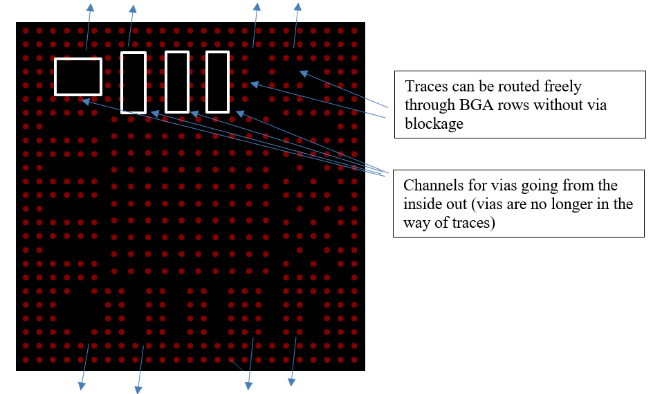
Via Channel Array Technology has been successfully used in a variety of TI products that help in minimizing package dimensions by using smaller ball pitch and low cost PCB routing. Via Channel technology is a way of enabling routing channels to escape innermost BGA positions. This allows several advantages. First, the via outside diameter (also known as the annular ring) can be larger than it normally would be if it had to be placed in between the BGAs in a tighter pitch, because all the vias are placed in special areas called via channels. This makes PCB manufacturing less expensive because larger vias are possible. Second, the vias are grouped in a radial pattern instead of a series of concentric rings around the middle of the chip, which is the case with normal BGA array PCB routing. The traces are more easily routed out of the inner parts of the chip because they are not restricted to the narrow paths in between many rows of vias. The unique outer row routing and the via channel inner routing are two important parts of this technology on the AM62Px. The AM62Px BGA Via Channel Array is shown in Figure 2-1.
 Figure 2-1 AM62Px BGA Array with Via Channels
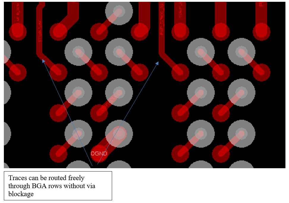
For the first two rows (from the outside in) of the BGA array, the balls have been arranged to allow wider traces than would otherwise be possible. The first row (the outside row) supports any size trace desired, because the trace comes from the PCB ball land and goes out on the PCB. Normally, the second row traces must be routed in between the first row of the PCB ball lands. The AM62Px allows escapes using a 4mil trace width/space on internal and external layers.
Figure 2-2 shows the first two rows of the AM62Px package and how it is possible to route 4 mil traces and spaces in the areas between balls.
 Figure 2-2 Outer Rows of Traces
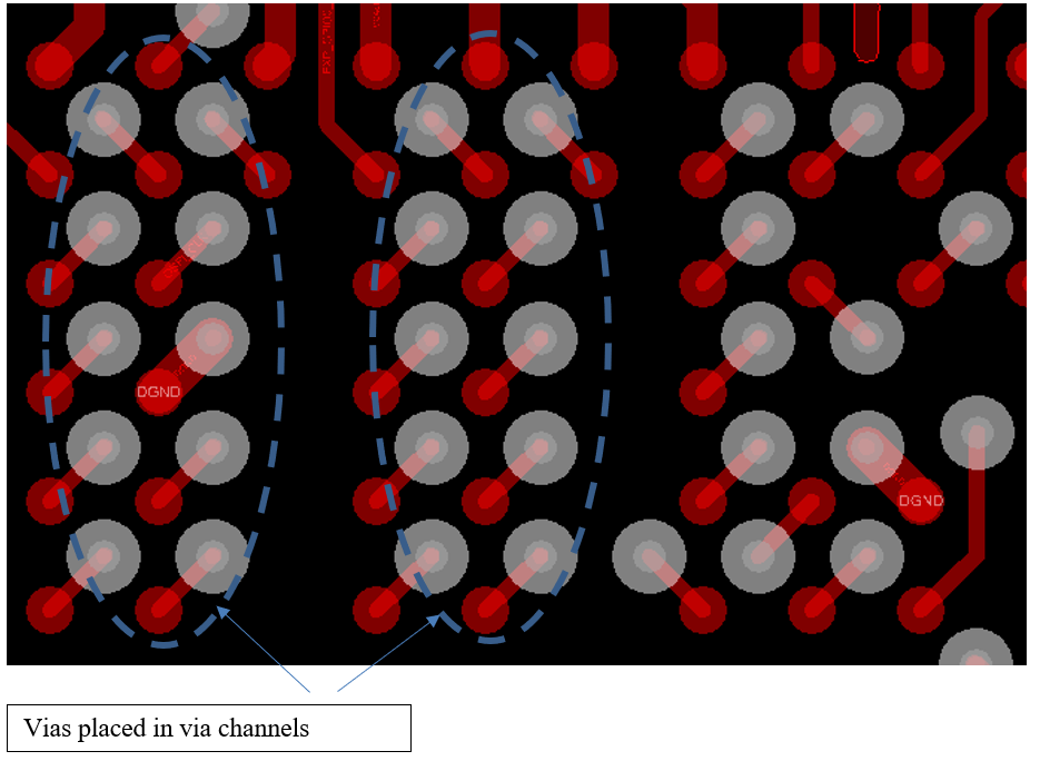
Starting at the third row, as with any BGA package, vias are necessary. As stated earlier, the vias are gathered in the via channels, so the only vias that must be placed in between balls are some of the power vias in areas of ground or power copper pour. In this case, they have no regular via ring because they are located in an area of copper pour where all the surrounding balls share the same net. This is elaborated more in later sections with details on via sharing. Because the via ring is larger than one that would normally fit in between these balls with the required clearance, the layout tool may flag a design rule check (DRC) error; however, this is a false warning because there is no risk of shorting to a nearby pad as they are all on the same net. The rest of the vias must be placed into the via channels as shown below. Figure 2-3 shows how the vias are grouped in the via channels.
 Figure 2-3 Vias in Via Channels