SPRADF0A November 2023 – November 2023 AM263P2 , AM263P4 , AM263P4-Q1
1 Why External on-PCB Flash?
MCU memory needs and CPU performance levels requirements are continuously increasing. MCU industry product roadmaps with up to 5K DMIPs and 64MB of on-chip flash are common, but it is well understood that embedded flash technologies are not expected to scale beyond 22 nm due to the high voltage (HV) gate oxide-based transistors required for programing and erasing flash bits. For example, on 28nm, 18 additional masks or reticles are required (vs. the CMOS only process technology).1, 2.
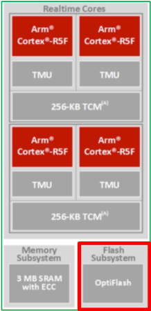
In comparison, typical 8MB Octal Serial Peripheral Interface (OSPI) flash can vary in cost from ~$0.50 - ~0.80. Figure 1-1 shows the AM263P CPU + TCM architecture with the flash sub-system (FSS) that includes OptiFlash.
 Figure 1-1 AM263P CPU + TCM
Architecture
Figure 1-1 AM263P CPU + TCM
ArchitectureThe additional cost of embedded flash technology results in either high-cost MCUs or architectures that reduce the amount of OCSRAM to achieve a specific cost point.
Since OCSRAM or TCM is always required for highly deterministic, low latency applications (such as real-time control), MCU architectures with a larger OCSRAM to Flash ration perform better. For example, the AM263P TCM has an access time of 2.5 ns and OCSRAM worst-case accesses can vary between 60 ns-90 ns.
Finally, alternative non-volatile memory (NVM) technologies such as, phase-change SRAM (PC-SRAM) or magnetic RAM (MRAM), are not yet ready for use in volume production of high reliability, low defective parts per million (DPPM) applications such as automotive and industrial.
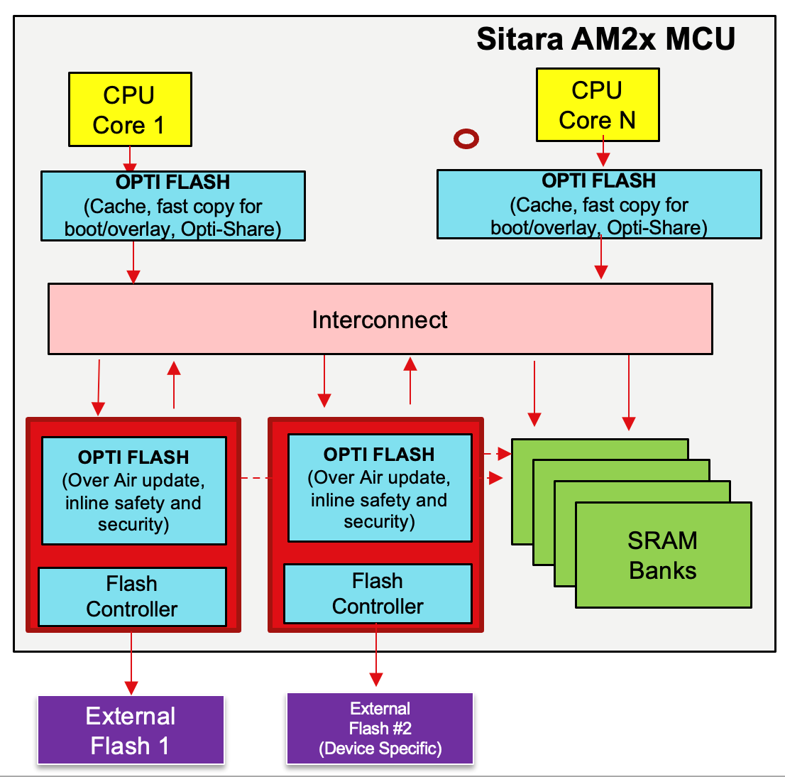
 Figure 1-2 OptiFlash Architecture Diagram