SPRADG4A January   2024  – April 2024


  1.   1
  2.   Abstract
  3.   Trademarks
  4. 1General Texas Instruments High Voltage Evaluation (TI HV EVM) User Safety Guidelines
  5. 2Introduction
  6. 3System Description
    1. 3.1 Key System Specifications
  7. 4System Overview
    1. 4.1 Block Diagram
    2. 4.2 Basic Operation
    3. 4.3 System Design Theory
      1. 4.3.1 Peak Current Mode Control (PCMC) Implementation
      2. 4.3.2 Zero Voltage Switching (ZVS) or Low Voltage Switching (LVS)
      3. 4.3.3 Synchronous Rectification
      4. 4.3.4 Slope Compensation
  8. 5Hardware
    1. 5.1 Hardware Overview
    2. 5.2 Hardware and Test Instruments Required
    3. 5.3 TMDSCNCD263 controlCARD™ Changes
  9. 6Software
    1. 6.1 Getting Started With Firmware
      1. 6.1.1 Opening the Code Composer Studio Project
      2. 6.1.2 Software Architecture
      3. 6.1.3 Project Folder Structure
    2. 6.2 SysConfig Setup
      1. 6.2.1 EPWM Configuration
      2. 6.2.2 ADC Configuration
      3. 6.2.3 CMPSS Configuration
    3. 6.3 Incremental Builds
      1. 6.3.1 Procedure for Running the Incremental Builds - PCMC
        1. 6.3.1.1 Lab 1: Phase Overlapping Check With Open Current and Voltage Loop
          1. 6.3.1.1.1 Objective of Lab 1
          2. 6.3.1.1.2 Overview of Lab 1
          3. 6.3.1.1.3 Procedure of Lab 1
            1. 6.3.1.1.3.1 Start CCS and Open a Project for Lab 1
            2. 6.3.1.1.3.2 Build and Load the Project for Lab 1
            3. 6.3.1.1.3.3 Debug Environment Windows for Lab 1
            4. 6.3.1.1.3.4 Run the Code for Lab 1
        2. 6.3.1.2 Lab 2: Closed Current and Open Voltage Loop
          1. 6.3.1.2.1 Objective of Lab 2
          2. 6.3.1.2.2 Overview of Lab 2
          3. 6.3.1.2.3 Procedure of Lab 2
            1. 6.3.1.2.3.1 Build and Load Project for Lab 2
            2. 6.3.1.2.3.2 Debug Environment Windows for Lab 2
            3. 6.3.1.2.3.3 Run the Code for Lab 2
        3. 6.3.1.3 Lab 3: Closed Current and Closed Voltage Loop
          1. 6.3.1.3.1 Objective of Lab 3
          2. 6.3.1.3.2 Overview of Lab 3
          3. 6.3.1.3.3 Procedure of Lab 3
            1. 6.3.1.3.3.1 Build and Load Project for Lab 3
            2. 6.3.1.3.3.2 Debug Environment Windows for Lab 3
            3. 6.3.1.3.3.3 Run the Code for Lab 3
  10. 7Testing and Results
    1. 7.1 Lab 0: Basic PWM Check
    2. 7.2 Lab 1: Phase Overlapping Check With Open Current and Voltage Loop
    3. 7.3 Lab 2: Closed Current and Open Voltage Loop
    4. 7.4 Lab 3: Closed Current and Closed Voltage Loop
  11. 8References
  12. 9Revision History
Overview of Lab 2

The software in lab 2 was configured so that the user can quickly evaluate the DAC driver module by viewing various waveforms on an oscilloscope and observing the effect of change in peak current reference command on the output voltage by interactively adjusting this command from CCS. The on-chip analog comparator compares the transformer primary current with the slope compensated peak current reference. Comparator output is connected to the trip zone logic of the PWM modules. ePWM4 module acts as the master time-base for the system. It operates in up-down count mode. ePWM4A and ePWM4B drive Q1 and Q4 full-bridge switches, while ePWM3A and ePWM3B drive Q2 and Q3 full-bridge switches. ePWM3A and ePWM3B drive Q5 and Q6 synchronous rectifier switches. Although the gating pulses for Q5 and Q6 are active, these switches do not start to operate unless 12V power supply is given to the base board through pin number 9 of J17 port. Whenever the comparator output goes high in a PWM half cycle, the ePWM3 module output (ePWM3A or ePWM3B) which was high at that instant is immediately pulled low while the other PWM3 module output is pulled high after an appropriate dead-band window (dbAtoP). ePWM5A and ePWM5B outputs are driven in a similar way. Note that this slope compensation ramp generation, comparator action and PWM waveform generation are all hardware generated without any software involvement as shown in Figure 6-9. Some register reconfigurations for SR are done inside the ISR.
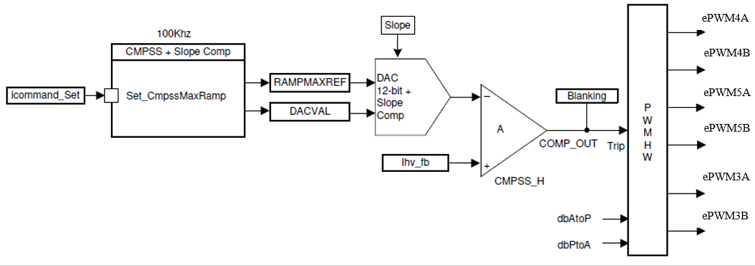
GUID-A79C1F79-4B07-405F-9376-C99BA2C863D1-low.png Figure 6-9 Lab 2 Software Blocks