SPRADG4A January 2024 – April 2024
- 1
- Abstract
- Trademarks
- 1General Texas Instruments High Voltage Evaluation (TI HV EVM) User Safety Guidelines
- 2Introduction
- 3System Description
- 4System Overview
- 5Hardware
-
6Software
- 6.1 Getting Started With Firmware
- 6.2 SysConfig Setup
- 6.3 Incremental Builds
- 7Testing and Results
- 8References
- 9Revision History
4.2 Basic Operation
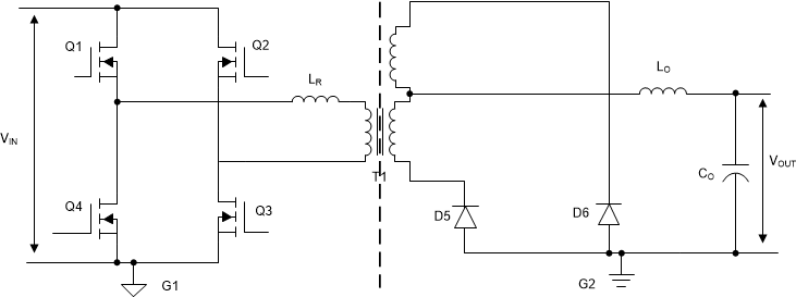
A PSFB converter consists of four-power electronic switches (like MOSFETs or IGBTs) that form a full-bridge on the primary side of the isolation transformer and diode rectifiers or MOSFET switches for synchronous rectification (SR) on the secondary side. This topology allows the switching devices to switch with zero voltage switching (ZVS) resulting in lower switching losses and an efficient converter.
For such an isolated topology, signal rectification is required on the secondary side. For systems with low output voltage and/or high output current ratings, implementing synchronous rectification instead of diode rectification achieves the best possible performance by avoiding diode rectification losses. In this work, synchronous rectification is implemented on the secondary side.
 Figure 4-2 A Phase-Shifted Full Bridge
Circuit
Figure 4-2 A Phase-Shifted Full Bridge
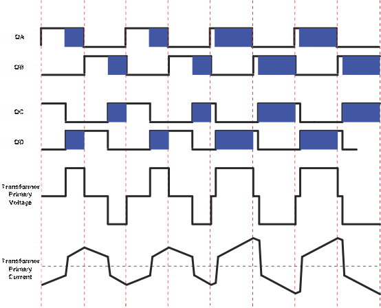
CircuitFigure 4-2 shows a simplified circuit of a phase shifted full-bridge. MOSFET switches Q1, Q4, Q2 and Q3 form the full-bridge on the primary side of the transformer T1. Q1 and Q4 are switched at 50 % duty and 180° out of phase with each other. Similarly, Q2 and Q3 are switched at 50 % duty and 180° out of phase with each other. The PWM switching signals for leg Q2 – Q3 of the full-bridge are phase shifted with respect to those for leg Q1 - Q4. Amount of this phase shift decides the amount of overlap between diagonal switches, which in turn decides the amount of energy transferred. D5, D6 provide diode rectification on the secondary(MOSFETs used in our design for SR), while Lo and Co form the output filter. Shim inductor LR provides assistance to the transformer leakage inductance for resonance operation with MOSFET capacitance and facilitates Zero Voltage Switching (ZVS). The switching waveforms for the system are shown in Figure 4-3.
 Figure 4-3 PSFB PWM Waveforms