SPRADG4A January   2024  – April 2024


  1.   1
  2.   Abstract
  3.   Trademarks
  4. 1General Texas Instruments High Voltage Evaluation (TI HV EVM) User Safety Guidelines
  5. 2Introduction
  6. 3System Description
    1. 3.1 Key System Specifications
  7. 4System Overview
    1. 4.1 Block Diagram
    2. 4.2 Basic Operation
    3. 4.3 System Design Theory
      1. 4.3.1 Peak Current Mode Control (PCMC) Implementation
      2. 4.3.2 Zero Voltage Switching (ZVS) or Low Voltage Switching (LVS)
      3. 4.3.3 Synchronous Rectification
      4. 4.3.4 Slope Compensation
  8. 5Hardware
    1. 5.1 Hardware Overview
    2. 5.2 Hardware and Test Instruments Required
    3. 5.3 TMDSCNCD263 controlCARD™ Changes
  9. 6Software
    1. 6.1 Getting Started With Firmware
      1. 6.1.1 Opening the Code Composer Studio Project
      2. 6.1.2 Software Architecture
      3. 6.1.3 Project Folder Structure
    2. 6.2 SysConfig Setup
      1. 6.2.1 EPWM Configuration
      2. 6.2.2 ADC Configuration
      3. 6.2.3 CMPSS Configuration
    3. 6.3 Incremental Builds
      1. 6.3.1 Procedure for Running the Incremental Builds - PCMC
        1. 6.3.1.1 Lab 1: Phase Overlapping Check With Open Current and Voltage Loop
          1. 6.3.1.1.1 Objective of Lab 1
          2. 6.3.1.1.2 Overview of Lab 1
          3. 6.3.1.1.3 Procedure of Lab 1
            1. 6.3.1.1.3.1 Start CCS and Open a Project for Lab 1
            2. 6.3.1.1.3.2 Build and Load the Project for Lab 1
            3. 6.3.1.1.3.3 Debug Environment Windows for Lab 1
            4. 6.3.1.1.3.4 Run the Code for Lab 1
        2. 6.3.1.2 Lab 2: Closed Current and Open Voltage Loop
          1. 6.3.1.2.1 Objective of Lab 2
          2. 6.3.1.2.2 Overview of Lab 2
          3. 6.3.1.2.3 Procedure of Lab 2
            1. 6.3.1.2.3.1 Build and Load Project for Lab 2
            2. 6.3.1.2.3.2 Debug Environment Windows for Lab 2
            3. 6.3.1.2.3.3 Run the Code for Lab 2
        3. 6.3.1.3 Lab 3: Closed Current and Closed Voltage Loop
          1. 6.3.1.3.1 Objective of Lab 3
          2. 6.3.1.3.2 Overview of Lab 3
          3. 6.3.1.3.3 Procedure of Lab 3
            1. 6.3.1.3.3.1 Build and Load Project for Lab 3
            2. 6.3.1.3.3.2 Debug Environment Windows for Lab 3
            3. 6.3.1.3.3.3 Run the Code for Lab 3
  10. 7Testing and Results
    1. 7.1 Lab 0: Basic PWM Check
    2. 7.2 Lab 1: Phase Overlapping Check With Open Current and Voltage Loop
    3. 7.3 Lab 2: Closed Current and Open Voltage Loop
    4. 7.4 Lab 3: Closed Current and Closed Voltage Loop
  11. 8References
  12. 9Revision History

Software Architecture

The project flow contains initialization of all the peripheral clocks and submodules of the system on a chip (SOC) using the AM263x SysConfig Tool and MCU_PLUS_SDK_AM263x. Initializing the Peripheral IPs used in this design like EPWM, ADC, CMPSS and so forth, are discussed in Section 6.2.

The Software contains one ISRs and one background task. The code flow is described in Figure 6-2. The ISR is scheduled to run every 10μs. It contains the main control loop explained in Section 4.3.1.
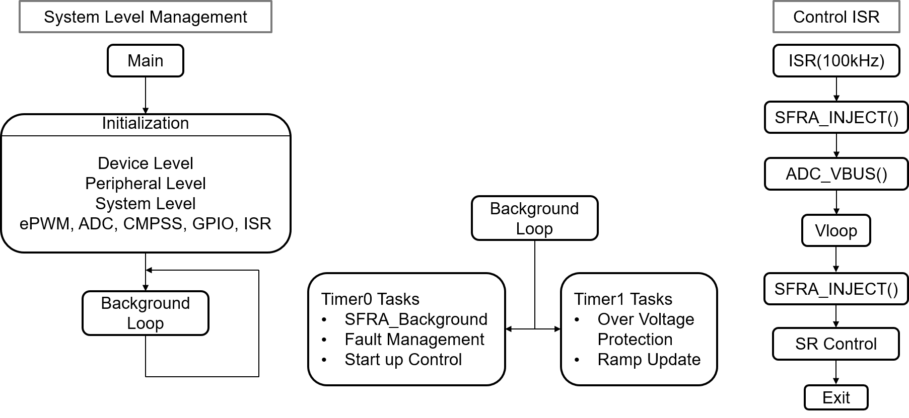
GUID-ABDB7294-F69E-4ADA-99A1-CD859BA18A30-low.png Figure 6-2 Software Block Diagram