SPRS951F December 2015 – May 2019 TDA2HF , TDA2HG , TDA2HV , TDA2LF , TDA2SA , TDA2SG , TDA2SX
PRODUCTION DATA.
- 1 Device Overview
- 2 Revision History
- 3 Device Comparison
-
4 Terminal Configuration and Functions
- 4.1 Terminal Assignment
- 4.2 Ball Characteristics
- 4.3 Multiplexing Characteristics
- 4.4
Signal Descriptions
- 4.4.1 Video Input Port (VIP)
- 4.4.2 Display Subsystem – Video Output Ports
- 4.4.3 Display Subsystem – High-Definition Multimedia Interface (HDMI)
- 4.4.4 External Memory Interface (EMIF)
- 4.4.5 General-Purpose Memory Controller (GPMC)
- 4.4.6 Timers
- 4.4.7 Inter-Integrated Circuit Interface (I2C)
- 4.4.8 Universal Asynchronous Receiver Transmitter (UART)
- 4.4.9 Multichannel Serial Peripheral Interface (McSPI)
- 4.4.10 Quad Serial Peripheral Interface (QSPI)
- 4.4.11 Multichannel Audio Serial Port (McASP)
- 4.4.12 Universal Serial Bus (USB)
- 4.4.13 SATA
- 4.4.14 Peripheral Component Interconnect Express (PCIe)
- 4.4.15 Controller Area Network Interface (DCAN)
- 4.4.16 Ethernet Interface (GMAC_SW)
- 4.4.17 eMMC/SD/SDIO
- 4.4.18 General-Purpose Interface (GPIO)
- 4.4.19 Pulse Width Modulation (PWM) Interface
- 4.4.20 System and Miscellaneous
- 4.4.21 Test Interfaces
-
5 Specifications
- 5.1 Absolute Maximum Ratings
- 5.2 ESD Ratings
- 5.3 Power on Hour (POH) Limits
- 5.4 Recommended Operating Conditions
- 5.5 Operating Performance Points
- 5.6 Power Consumption Summary
- 5.7
Electrical Characteristics
- 5.7.1 LVCMOS DDR DC Electrical Characteristics
- 5.7.2 HDMIPHY DC Electrical Characteristics
- 5.7.3 Dual Voltage LVCMOS I2C DC Electrical Characteristics
- 5.7.4 IQ1833 Buffers DC Electrical Characteristics
- 5.7.5 IHHV1833 Buffers DC Electrical Characteristics
- 5.7.6 LVCMOS OSC Buffers DC Electrical Characteristics
- 5.7.7 BC1833IHHV Buffers DC Electrical Characteristics
- 5.7.8 USBPHY DC Electrical Characteristics
- 5.7.9 Dual Voltage SDIO1833 DC Electrical Characteristics
- 5.7.10 Dual Voltage LVCMOS DC Electrical Characteristics
- 5.7.11 SATAPHY DC Electrical Characteristics
- 5.7.12 PCIEPHY DC Electrical Characteristics
- 5.8 Thermal Resistance Characteristics
- 5.9 Power Supply Sequences
- 6 Clock Specifications
-
7 Timing Requirements and Switching Characteristics
- 7.1 Timing Test Conditions
- 7.2 Interface Clock Specifications
- 7.3 Timing Parameters and Information
- 7.4 Recommended Clock and Control Signal Transition Behavior
- 7.5 Virtual and Manual I/O Timing Modes
- 7.6 Video Input Ports (VIP)
- 7.7 Display Subsystem – Video Output Ports
- 7.8 Display Subsystem – High-Definition Multimedia Interface (HDMI)
- 7.9 External Memory Interface (EMIF)
- 7.10 General-Purpose Memory Controller (GPMC)
- 7.11 Timers
- 7.12 Inter-Integrated Circuit Interface (I2C)
- 7.13 Universal Asynchronous Receiver Transmitter (UART)
- 7.14 Multichannel Serial Peripheral Interface (McSPI)
- 7.15 Quad Serial Peripheral Interface (QSPI)
- 7.16
Multichannel Audio Serial Port (McASP)
- Table 7-45 Timing Requirements for McASP1
- Table 7-46 Timing Requirements for McASP2
- Table 7-47 Timing Requirements for McASP3/4/5/6/7/8
- Table 7-48 Switching Characteristics Over Recommended Operating Conditions for McASP1
- Table 7-49 Switching Characteristics Over Recommended Operating Conditions for McASP2
- Table 7-50 Switching Characteristics Over Recommended Operating Conditions for McASP3/4/5/6/7/8
- 7.17 Universal Serial Bus (USB)
- 7.18 Serial Advanced Technology Attachment (SATA)
- 7.19 Peripheral Component Interconnect Express (PCIe)
- 7.20 Controller Area Network Interface (DCAN)
- 7.21
Ethernet Interface (GMAC_SW)
- 7.21.1
GMAC MII Timings
- Table 7-67 Timing Requirements for miin_rxclk - MII Operation
- Table 7-68 Timing Requirements for miin_txclk - MII Operation
- Table 7-69 Timing Requirements for GMAC MIIn Receive 10/100 Mbit/s
- Table 7-70 Switching Characteristics Over Recommended Operating Conditions for GMAC MIIn Transmit 10/100 Mbits/s
- 7.21.2 GMAC MDIO Interface Timings
- 7.21.3
GMAC RMII Timings
- Table 7-75 Timing Requirements for GMAC REF_CLK - RMII Operation
- Table 7-76 Timing Requirements for GMAC RMIIn Receive
- Table 7-77 Switching Characteristics Over Recommended Operating Conditions for GMAC REF_CLK - RMII Operation
- Table 7-78 Switching Characteristics Over Recommended Operating Conditions for GMAC RMIIn Transmit 10/100 Mbits/s
- 7.21.4
GMAC RGMII Timings
- Table 7-82 Timing Requirements for rgmiin_rxc - RGMIIn Operation
- Table 7-83 Timing Requirements for GMAC RGMIIn Input Receive for 10/100/1000 Mbps
- Table 7-84 Switching Characteristics Over Recommended Operating Conditions for rgmiin_txctl - RGMIIn Operation for 10/100/1000 Mbit/s
- Table 7-85 Switching Characteristics for GMAC RGMIIn Output Transmit for 10/100/1000 Mbps
- 7.21.1
GMAC MII Timings
- 7.22
eMMC/SD/SDIO
- 7.22.1
MMC1—SD Card Interface
- 7.22.1.1 Default speed, 4-bit data, SDR, half-cycle
- 7.22.1.2 High speed, 4-bit data, SDR, half-cycle
- 7.22.1.3 SDR12, 4-bit data, half-cycle
- 7.22.1.4 SDR25, 4-bit data, half-cycle
- 7.22.1.5 UHS-I SDR50, 4-bit data, half-cycle
- 7.22.1.6 UHS-I SDR104, 4-bit data, half-cycle
- 7.22.1.7 UHS-I DDR50, 4-bit data
- 7.22.2 MMC2 — eMMC
- 7.22.3 MMC3 and MMC4—SDIO/SD
- 7.22.1
MMC1—SD Card Interface
- 7.23 General-Purpose Interface (GPIO)
- 7.24 System and Miscellaneous interfaces
- 7.25
Test Interfaces
- 7.25.1
IEEE 1149.1 Standard-Test-Access Port (JTAG)
- 7.25.1.1
JTAG Electrical Data/Timing
- Table 7-134 Timing Requirements for IEEE 1149.1 JTAG
- Table 7-135 Switching Characteristics Over Recommended Operating Conditions for IEEE 1149.1 JTAG
- Table 7-136 Timing Requirements for IEEE 1149.1 JTAG With RTCK
- Table 7-137 Switching Characteristics Over Recommended Operating Conditions for IEEE 1149.1 JTAG With RTCK
- 7.25.1.1
JTAG Electrical Data/Timing
- 7.25.2 Trace Port Interface Unit (TPIU)
- 7.25.1
IEEE 1149.1 Standard-Test-Access Port (JTAG)
-
8 Applications, Implementation, and Layout
- 8.1 Introduction
- 8.2 Power Optimizations
- 8.3 Core Power Domains
- 8.4 Single-Ended Interfaces
- 8.5
Differential Interfaces
- 8.5.1 General Routing Guidelines
- 8.5.2
USB 2.0 Board Design and Layout Guidelines
- 8.5.2.1 Background
- 8.5.2.2
USB PHY Layout Guide
- 8.5.2.2.1 General Routing and Placement
- 8.5.2.2.2
Specific Guidelines for USB PHY Layout
- 8.5.2.2.2.1 Analog, PLL, and Digital Power Supply Filtering
- 8.5.2.2.2.2 Analog, Digital, and PLL Partitioning
- 8.5.2.2.2.3 Board Stackup
- 8.5.2.2.2.4 Cable Connector Socket
- 8.5.2.2.2.5 Clock Routings
- 8.5.2.2.2.6 Crystals/Oscillator
- 8.5.2.2.2.7 DP/DM Trace
- 8.5.2.2.2.8 DP/DM Vias
- 8.5.2.2.2.9 Image Planes
- 8.5.2.2.2.10 JTAG Interface
- 8.5.2.2.2.11 Power Regulators
- 8.5.2.3 Electrostatic Discharge (ESD)
- 8.5.2.4 References
- 8.5.3 USB 3.0 Board Design and Layout Guidelines
- 8.5.4 HDMI Board Design and Layout Guidelines
- 8.5.5 SATA Board Design and Layout Guidelines
- 8.5.6 PCIe Board Design and Layout Guidelines
- 8.6 Clock Routing Guidelines
- 8.7
DDR2/DDR3 Board Design and Layout Guidelines
- 8.7.1 DDR2/DDR3 General Board Layout Guidelines
- 8.7.2 DDR2 Board Design and Layout Guidelines
- 8.7.3
DDR3 Board Design and Layout Guidelines
- 8.7.3.1 Board Designs
- 8.7.3.2 DDR3 EMIFs
- 8.7.3.3 DDR3 Device Combinations
- 8.7.3.4 DDR3 Interface Schematic
- 8.7.3.5 Compatible JEDEC DDR3 Devices
- 8.7.3.6 PCB Stackup
- 8.7.3.7 Placement
- 8.7.3.8 DDR3 Keepout Region
- 8.7.3.9 Bulk Bypass Capacitors
- 8.7.3.10 High-Speed Bypass Capacitors
- 8.7.3.11 Net Classes
- 8.7.3.12 DDR3 Signal Termination
- 8.7.3.13 VREF_DDR Routing
- 8.7.3.14 VTT
- 8.7.3.15 CK and ADDR_CTRL Topologies and Routing Definition
- 8.7.3.16 Data Topologies and Routing Definition
- 8.7.3.17 Routing Specification
- 9 Device and Documentation Support
- 10Mechanical, Packaging, and Orderable Information
8.7.2.3 DDR2 CK and ADDR_CTRL Routing
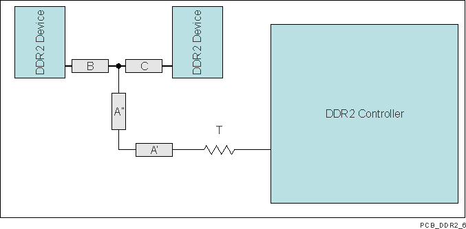
Figure 8-55 shows the topology of the routing for the CK and ADDR_CTRL net classes. The route is a balanced T as it is intended that the length of segments B and C be equal. In addition, the length of A = (A'+A'') should be maximized.
 Figure 8-55 CK and ADDR_CTRL Routing and Topology
 Table 8-40 CK and ADDR_CTRL Routing Specification (1)
| NO. | PARAMETER | MIN | MAX | UNIT |
|---|---|---|---|---|
| RSC21 | Center-to-center ddrx_ck - ddrx_nck spacing | 2w | ||
| RSC22 | ddrx_ck / ddrx_nck skew(1) | 5 | ps | |
| RSC23 | CK A-to-B/A-to-C skew mismatch(2) | 10 | ps | |
| RSC24 | CK B-to-C skew mismatch | 10 | ps | |
| RSC25 | Center-to-center CK to other DDR2 trace spacing(3) | 4w | ||
| RSC26 | CK/ADDR_CTRL trace length(4) | 680 | ps | |
| RSC27 | ADDR_CTRL-to-CK skew mismatch | 25 | ps | |
| RSC28 | ADDR_CTRL-to-ADDR_CTRL skew mismatch | 25 | ps | |
| RSC29 | Center-to-center ADDR_CTRL to other DDR2 trace spacing(3) | 4w | ||
| RSC210 | Center-to-center ADDR_CTRL to other ADDR_CTRL trace spacing(3) | 3w | ||
| RSC211 | ADDR_CTRL A-to-B/A-to-C skew mismatch(2) | 25 | ps | |
| RSC212 | ADDR_CTRL B-to-C skew mismatch | 25 | ps |
- The length of segment A = A' + A′′ as shown in Figure 8-55.
- Series terminator, if used, should be located closest to the Device.
- Center-to-center spacing is allowed to fall to minimum 2w for up to 500 mils of routed length to accommodate BGA escape and routing congestion.
- This is the longest routing length of the CK and ADDR_CTRL net classes.
- Length of A should be maximized.
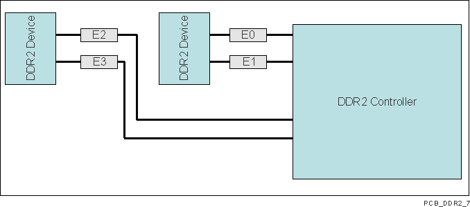
Figure 8-56 shows the topology and routing for the DQS and DQ net classes; the routes are point to point. Skew matching across bytes is not needed nor recommended.
 Figure 8-56 DQS and DQ Routing and Topology
 Table 8-41 DQS and DQ Routing Specification
| NO. | PARAMETER | MIN | MAX | UNIT |
|---|---|---|---|---|
| RSDQ21 | Center-to-center DQS-DQSn spacing in E0|E1|E2|E3 | 2w | ||
| RSDQ22 | DQS-DQSn skew in E0|E1|E2|E3 | 5 | ps | |
| RSDQ23 | Center-to-center DQS to other DDR2 trace spacing(1) | 4w | ||
| RSDQ24 | DQS/DQ trace length (2)(3)(4) | 325 | ps | |
| RSDQ25 | DQ-to-DQS skew mismatch(2)(3)(4) | 10 | ps | |
| RSDQ26 | DQ-to-DQ skew mismatch(2)(3)(4) | 10 | ps | |
| RSDQ27 | DQ-to-DQ/DQS via count mismatch(2)(3)(4) | 1 | Vias | |
| RSDQ28 | Center-to-center DQ to other DDR2 trace spacing(1)(5) | 4w | ||
| RSDQ29 | Center-to-center DQ to other DQ trace spacing(1)(6)(7) | 3w | ||
| RSDQ210 | DQ/DQS E skew mismatch(2)(3)(4) | 25 | ps |
- Center-to-center spacing is allowed to fall to minimum 2w for up to 500 mils of routed length to accommodate BGA escape and routing congestion.
- A 16-bit DDR memory system has two sets of data net classes; one for data byte 0, and one for data byte 1, each with an associated DQS (2 DQSs) per DDR EMIF used.
- A 32-bit DDR memory system has four sets of data net classes; one each for data bytes 0 through 3, and each associated with a DQS (4 DQSs) per DDR EMIF used.
- There is no need, and it is not recommended, to skew match across data bytes; that is, from DQS0 and data byte 0 to DQS1 and data byte 1.
- DQs from other DQS domains are considered other DDR2 trace.
- DQs from other data bytes are considered other DDR2 trace.
- This is the longest routing distance of each of the DQS and DQ net classes.