SPRSP45C March   2020  – April 2024 TMS320F280021 , TMS320F280021-Q1 , TMS320F280023 , TMS320F280023-Q1 , TMS320F280023C , TMS320F280025 , TMS320F280025-Q1 , TMS320F280025C , TMS320F280025C-Q1

PRODUCTION DATA  

  1.   1
  2. Features
  3. Applications
  4. Description
    1. 3.1 Functional Block Diagram
  5. Device Comparison
    1. 4.1 Related Products
  6. Terminal Configuration and Functions
    1. 5.1 Pin Diagrams
    2. 5.2 Pin Attributes
    3. 5.3 Signal Descriptions
      1. 5.3.1 Analog Signals
      2. 5.3.2 Digital Signals
      3. 5.3.3 Power and Ground
      4. 5.3.4 Test, JTAG, and Reset
    4. 5.4 Pin Multiplexing
      1. 5.4.1 GPIO Muxed Pins
        1. 5.4.1.1 GPIO Muxed Pins Table
      2. 5.4.2 Digital Inputs on ADC Pins (AIOs)
      3. 5.4.3 GPIO Input X-BAR
      4. 5.4.4 GPIO Output X-BAR, CLB X-BAR, CLB Output X-BAR, and ePWM X-BAR
    5. 5.5 Pins With Internal Pullup and Pulldown
    6. 5.6 Connections for Unused Pins
  7. Specifications
    1. 6.1  Absolute Maximum Ratings
    2. 6.2  ESD Ratings – Commercial
    3. 6.3  ESD Ratings – Automotive
    4. 6.4  Recommended Operating Conditions
    5.     Supply Voltages
    6. 6.5  Power Consumption Summary
      1. 6.5.1 System Current Consumption
      2. 6.5.2 Operating Mode Test Description
      3. 6.5.3 Current Consumption Graphs
      4. 6.5.4 Reducing Current Consumption
        1. 6.5.4.1 Typical Current Reduction per Disabled Peripheral
    7. 6.6  Electrical Characteristics
    8. 6.7  Thermal Resistance Characteristics for PN Package
    9. 6.8  Thermal Resistance Characteristics for PM Package
    10. 6.9  Thermal Resistance Characteristics for PT Package
    11. 6.10 Thermal Design Considerations
    12. 6.11 System
      1. 6.11.1  Power Management Module (PMM)
        1. 6.11.1.1 Introduction
        2. 6.11.1.2 Overview
          1. 6.11.1.2.1 Power Rail Monitors
            1. 6.11.1.2.1.1 I/O POR (Power-On Reset) Monitor
            2. 6.11.1.2.1.2 I/O BOR (Brown-Out Reset) Monitor
            3. 6.11.1.2.1.3 VDD POR (Power-On Reset) Monitor
          2. 6.11.1.2.2 External Supervisor Usage
          3. 6.11.1.2.3 Delay Blocks
          4. 6.11.1.2.4 Internal 1.2-V LDO Voltage Regulator (VREG)
        3. 6.11.1.3 External Components
          1. 6.11.1.3.1 Decoupling Capacitors
            1. 6.11.1.3.1.1 VDDIO Decoupling
            2. 6.11.1.3.1.2 VDD Decoupling
        4. 6.11.1.4 Power Sequencing
          1. 6.11.1.4.1 Supply Pins Ganging
          2. 6.11.1.4.2 Signal Pins Power Sequence
          3. 6.11.1.4.3 Supply Pins Power Sequence
            1. 6.11.1.4.3.1 Internal VREG/VDD Mode Sequence
            2. 6.11.1.4.3.2 Supply Sequencing Summary and Effects of Violations
            3. 6.11.1.4.3.3 Supply Slew Rate
        5. 6.11.1.5 Power Management Module Electrical Data and Timing
          1. 6.11.1.5.1 Power Management Module Characteristics
          2. 6.11.1.5.2 Power Management Module Operating Conditions
      2. 6.11.2  Reset Timing
        1. 6.11.2.1 Reset Sources
        2. 6.11.2.2 Reset Electrical Data and Timing
          1. 6.11.2.2.1 Reset (XRSn) Timing Requirements
          2. 6.11.2.2.2 Reset (XRSn) Switching Characteristics
          3. 6.11.2.2.3 Reset Timing Diagrams
      3. 6.11.3  Clock Specifications
        1. 6.11.3.1 Clock Sources
        2. 6.11.3.2 Clock Frequencies, Requirements, and Characteristics
          1. 6.11.3.2.1 Input Clock Frequency and Timing Requirements, PLL Lock Times
            1. 6.11.3.2.1.1 Input Clock Frequency
            2. 6.11.3.2.1.2 XTAL Oscillator Characteristics
            3. 6.11.3.2.1.3 X1 Timing Requirements
            4. 6.11.3.2.1.4 APLL Characteristics
            5. 6.11.3.2.1.5 XCLKOUT Switching Characteristics
            6. 6.11.3.2.1.6 Internal Clock Frequencies
        3. 6.11.3.3 Input Clocks and PLLs
        4. 6.11.3.4 XTAL Oscillator
          1. 6.11.3.4.1 Introduction
          2. 6.11.3.4.2 Overview
            1. 6.11.3.4.2.1 Electrical Oscillator
              1. 6.11.3.4.2.1.1 Modes of Operation
                1. 6.11.3.4.2.1.1.1 Crystal Mode of Operation
                2. 6.11.3.4.2.1.1.2 Single-Ended Mode of Operation
              2. 6.11.3.4.2.1.2 XTAL Output on XCLKOUT
            2. 6.11.3.4.2.2 Quartz Crystal
            3. 6.11.3.4.2.3 GPIO Modes of Operation
          3. 6.11.3.4.3 Functional Operation
            1. 6.11.3.4.3.1 ESR – Effective Series Resistance
            2. 6.11.3.4.3.2 Rneg – Negative Resistance
            3. 6.11.3.4.3.3 Start-up Time
            4. 6.11.3.4.3.4 DL – Drive Level
          4. 6.11.3.4.4 How to Choose a Crystal
          5. 6.11.3.4.5 Testing
          6. 6.11.3.4.6 Common Problems and Debug Tips
          7. 6.11.3.4.7 Crystal Oscillator Specifications
            1. 6.11.3.4.7.1 Crystal Oscillator Electrical Characteristics
            2. 6.11.3.4.7.2 Crystal Equivalent Series Resistance (ESR) Requirements
        5. 6.11.3.5 Internal Oscillators
          1. 6.11.3.5.1 INTOSC Characteristics
      4. 6.11.4  Flash Parameters
      5. 6.11.5  RAM Specifications
      6. 6.11.6  ROM Specifications
      7. 6.11.7  Emulation/JTAG
        1. 6.11.7.1 JTAG Electrical Data and Timing
          1. 6.11.7.1.1 JTAG Timing Requirements
          2. 6.11.7.1.2 JTAG Switching Characteristics
          3. 6.11.7.1.3 JTAG Timing Diagram
        2. 6.11.7.2 cJTAG Electrical Data and Timing
          1. 6.11.7.2.1 cJTAG Timing Requirements
          2. 6.11.7.2.2 cJTAG Switching Characteristics
          3. 6.11.7.2.3 cJTAG Timing Diagram
      8. 6.11.8  GPIO Electrical Data and Timing
        1. 6.11.8.1 GPIO – Output Timing
          1. 6.11.8.1.1 General-Purpose Output Switching Characteristics
        2. 6.11.8.2 GPIO – Input Timing
          1. 6.11.8.2.1 General-Purpose Input Timing Requirements
          2. 6.11.8.2.2 Sampling Mode
        3. 6.11.8.3 Sampling Window Width for Input Signals
      9. 6.11.9  Interrupts
        1. 6.11.9.1 External Interrupt (XINT) Electrical Data and Timing
          1. 6.11.9.1.1 External Interrupt Timing Requirements
          2. 6.11.9.1.2 External Interrupt Switching Characteristics
          3. 6.11.9.1.3 External Interrupt Timing
      10. 6.11.10 Low-Power Modes
        1. 6.11.10.1 Clock-Gating Low-Power Modes
        2. 6.11.10.2 Low-Power Mode Wake-up Timing
          1. 6.11.10.2.1 IDLE Mode Timing Requirements
          2. 6.11.10.2.2 IDLE Mode Switching Characteristics
          3. 6.11.10.2.3 IDLE Entry and Exit Timing Diagram
          4. 6.11.10.2.4 STANDBY Mode Timing Requirements
          5. 6.11.10.2.5 STANDBY Mode Switching Characteristics
          6. 6.11.10.2.6 STANDBY Entry and Exit Timing Diagram
          7. 6.11.10.2.7 HALT Mode Timing Requirements
          8. 6.11.10.2.8 HALT Mode Switching Characteristics
          9. 6.11.10.2.9 HALT Entry and Exit Timing Diagram
    13. 6.12 Analog Peripherals
      1. 6.12.1 Analog Pins and Internal Connections
      2. 6.12.2 Analog Signal Descriptions
      3. 6.12.3 Analog-to-Digital Converter (ADC)
        1. 6.12.3.1 ADC Configurability
          1. 6.12.3.1.1 Signal Mode
        2. 6.12.3.2 ADC Electrical Data and Timing
          1. 6.12.3.2.1 ADC Operating Conditions
          2. 6.12.3.2.2 ADC Characteristics
          3. 6.12.3.2.3 ADC INL and DNL
          4. 6.12.3.2.4 ADC Input Model
          5. 6.12.3.2.5 ADC Timing Diagrams
      4. 6.12.4 Temperature Sensor
        1. 6.12.4.1 Temperature Sensor Electrical Data and Timing
          1. 6.12.4.1.1 Temperature Sensor Characteristics
      5. 6.12.5 Comparator Subsystem (CMPSS)
        1. 6.12.5.1 CMPSS Electrical Data and Timing
          1. 6.12.5.1.1 Comparator Electrical Characteristics
          2.        CMPSS Comparator Input Referred Offset and Hysteresis
          3. 6.12.5.1.2 CMPSS DAC Static Electrical Characteristics
          4. 6.12.5.1.3 CMPSS Illustrative Graphs
    14. 6.13 Control Peripherals
      1. 6.13.1 Enhanced Pulse Width Modulator (ePWM)
        1. 6.13.1.1 Control Peripherals Synchronization
        2. 6.13.1.2 ePWM Electrical Data and Timing
          1. 6.13.1.2.1 ePWM Timing Requirements
          2. 6.13.1.2.2 ePWM Switching Characteristics
          3. 6.13.1.2.3 Trip-Zone Input Timing
            1. 6.13.1.2.3.1 Trip-Zone Input Timing Requirements
        3. 6.13.1.3 External ADC Start-of-Conversion Electrical Data and Timing
          1. 6.13.1.3.1 External ADC Start-of-Conversion Switching Characteristics
      2. 6.13.2 High-Resolution Pulse Width Modulator (HRPWM)
        1. 6.13.2.1 HRPWM Electrical Data and Timing
          1. 6.13.2.1.1 High-Resolution PWM Characteristics
      3. 6.13.3 Enhanced Capture and High-Resolution Capture (eCAP, HRCAP)
        1. 6.13.3.1 High-Resolution Capture (HRCAP)
        2. 6.13.3.2 eCAP and HRCAP Block Diagram
        3. 6.13.3.3 eCAP/HRCAP Synchronization
        4. 6.13.3.4 eCAP Electrical Data and Timing
          1. 6.13.3.4.1 eCAP Timing Requirements
          2. 6.13.3.4.2 eCAP Switching Characteristics
        5. 6.13.3.5 HRCAP Electrical Data and Timing
          1. 6.13.3.5.1 HRCAP Switching Characteristics
          2. 6.13.3.5.2 HRCAP Figure and Graph
      4. 6.13.4 Enhanced Quadrature Encoder Pulse (eQEP)
        1. 6.13.4.1 eQEP Electrical Data and Timing
          1. 6.13.4.1.1 eQEP Timing Requirements
          2. 6.13.4.1.2 eQEP Switching Characteristics
    15. 6.14 Communications Peripherals
      1. 6.14.1 Controller Area Network (CAN)
      2. 6.14.2 Inter-Integrated Circuit (I2C)
        1. 6.14.2.1 I2C Electrical Data and Timing
          1. 6.14.2.1.1 I2C Timing Requirements
          2. 6.14.2.1.2 I2C Switching Characteristics
          3. 6.14.2.1.3 I2C Timing Diagram
      3. 6.14.3 Power Management Bus (PMBus) Interface
        1. 6.14.3.1 PMBus Electrical Data and Timing
          1. 6.14.3.1.1 PMBus Electrical Characteristics
          2. 6.14.3.1.2 PMBus Fast Mode Switching Characteristics
          3. 6.14.3.1.3 PMBus Standard Mode Switching Characteristics
      4. 6.14.4 Serial Communications Interface (SCI)
      5. 6.14.5 Serial Peripheral Interface (SPI)
        1. 6.14.5.1 SPI Master Mode Timings
          1. 6.14.5.1.1 SPI Master Mode Timing Requirements
          2. 6.14.5.1.2 SPI Master Mode Switching Characteristics (Clock Phase = 0)
          3. 6.14.5.1.3 SPI Master Mode Switching Characteristics (Clock Phase = 1)
          4. 6.14.5.1.4 SPI Master Mode Timing Diagrams
        2. 6.14.5.2 SPI Slave Mode Timings
          1. 6.14.5.2.1 SPI Slave Mode Timing Requirements
          2. 6.14.5.2.2 SPI Slave Mode Switching Characteristics
          3. 6.14.5.2.3 SPI Slave Mode Timing Diagrams
      6. 6.14.6 Local Interconnect Network (LIN)
      7. 6.14.7 Fast Serial Interface (FSI)
        1. 6.14.7.1 FSI Transmitter
          1. 6.14.7.1.1 FSITX Electrical Data and Timing
            1. 6.14.7.1.1.1 FSITX Switching Characteristics
            2. 6.14.7.1.1.2 FSITX Timings
        2. 6.14.7.2 FSI Receiver
          1. 6.14.7.2.1 FSIRX Electrical Data and Timing
            1. 6.14.7.2.1.1 FSIRX Timing Requirements
            2. 6.14.7.2.1.2 FSIRX Switching Characteristics
            3. 6.14.7.2.1.3 FSIRX Timings
        3. 6.14.7.3 FSI SPI Compatibility Mode
          1. 6.14.7.3.1 FSITX SPI Signaling Mode Electrical Data and Timing
            1. 6.14.7.3.1.1 FSITX SPI Signaling Mode Switching Characteristics
            2. 6.14.7.3.1.2 FSITX SPI Signaling Mode Timings
      8. 6.14.8 Host Interface Controller (HIC)
        1. 6.14.8.1 HIC Electrical Data and Timing
          1. 6.14.8.1.1 HIC Timing Requirements
          2. 6.14.8.1.2 HIC Switching Characteristics
          3. 6.14.8.1.3 HIC Timing Diagrams
  8. Detailed Description
    1. 7.1  Overview
    2. 7.2  Functional Block Diagram
    3. 7.3  Memory
      1. 7.3.1 Memory Map
        1. 7.3.1.1 Dedicated RAM (Mx RAM)
        2. 7.3.1.2 Local Shared RAM (LSx RAM)
        3. 7.3.1.3 Global Shared RAM (GSx RAM)
      2. 7.3.2 Flash Memory Map
        1. 7.3.2.1 Addresses of Flash Sectors
      3. 7.3.3 Peripheral Registers Memory Map
    4. 7.4  Identification
    5. 7.5  Bus Architecture – Peripheral Connectivity
    6. 7.6  C28x Processor
      1. 7.6.1 Floating-Point Unit (FPU)
      2. 7.6.2 Fast Integer Division Unit
      3. 7.6.3 Trigonometric Math Unit (TMU)
      4. 7.6.4 VCRC Unit
    7. 7.7  Embedded Real-Time Analysis and Diagnostic (ERAD)
    8. 7.8  Background CRC-32 (BGCRC)
    9. 7.9  Direct Memory Access (DMA)
    10. 7.10 Device Boot Modes
      1. 7.10.1 Device Boot Configurations
        1. 7.10.1.1 Configuring Boot Mode Pins
        2. 7.10.1.2 Configuring Boot Mode Table Options
      2. 7.10.2 GPIO Assignments
    11. 7.11 Dual Code Security Module
    12. 7.12 Watchdog
    13. 7.13 C28x Timers
    14. 7.14 Dual-Clock Comparator (DCC)
      1. 7.14.1 Features
      2. 7.14.2 Mapping of DCCx (DCC0 and DCC1) Clock Source Inputs
    15. 7.15 Configurable Logic Block (CLB)
  9. Applications, Implementation, and Layout
    1. 8.1 Key Device Features
    2. 8.2 Application Information
      1. 8.2.1 Typical Application
        1. 8.2.1.1 Servo Drive Control Module
          1. 8.2.1.1.1 System Block Diagram
          2. 8.2.1.1.2 Servo Drive Control Module Resources
        2. 8.2.1.2 Server or Telecom Power Supply Unit (PSU)
          1. 8.2.1.2.1 System Block Diagram
          2. 8.2.1.2.2 Server and Telecom PSU Resources
        3. 8.2.1.3 Merchant Telecom Rectifiers
          1. 8.2.1.3.1 System Block Diagram
          2. 8.2.1.3.2 Merchant Telecom Rectifiers Resources
        4. 8.2.1.4 EV Charging Station Power Module
          1. 8.2.1.4.1 System Block Diagram
          2. 8.2.1.4.2 EV Charging Station Power Module Resources
        5. 8.2.1.5 Air-conditioner Outdoor Unit
          1. 8.2.1.5.1 System Block Diagram
          2. 8.2.1.5.2 Air Conditioner Outdoor Unit Resources
  10. Device and Documentation Support
    1. 9.1 Getting Started and Next Steps
    2. 9.2 Device and Development Support Tool Nomenclature
    3. 9.3 Markings
    4. 9.4 Tools and Software
    5. 9.5 Documentation Support
    6. 9.6 Support Resources
    7. 9.7 Trademarks
    8. 9.8 Electrostatic Discharge Caution
    9. 9.9 Glossary
  11. 10Revision History
  12. 11Mechanical, Packaging, and Orderable Information
    1. 11.1 Packaging Information
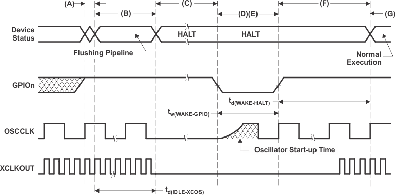
HALT Entry and Exit Timing Diagram
GUID-0BBC47D3-0F05-428B-B445-9BAC6B699EE7-low.gif
IDLE instruction is executed to put the device into HALT mode.
The LPM block responds to the HALT signal, SYSCLK is held for a maximum 16 INTOSC1 clock cycles before being turned off. This delay enables the CPU pipeline and any other pending operations to flush properly.
Clocks to the peripherals are turned off and the PLL is shut down. If a quartz crystal or ceramic resonator is used as the clock source, the internal oscillator is shut down as well. The device is now in HALT mode and consumes very little power. It is possible to keep the zero-pin internal oscillators (INTOSC1 and INTOSC2) and the watchdog alive in HALT MODE. This is done by writing 1 to CLKSRCCTL1.WDHALTI. After the IDLE instruction is executed, a delay of five OSCCLK cycles (minimum) is needed before the wake-up signal could be asserted.
When the GPIOn pin (used to bring the device out of HALT) is driven low, the oscillator is turned on and the oscillator wake-up sequence is initiated. The GPIO pin should be driven high only after the oscillator has stabilized. This enables the provision of a clean clock signal during the PLL lock sequence. Because the falling edge of the GPIO pin asynchronously begins the wake-up procedure, care should be taken to maintain a low noise environment before entering and during HALT mode.
The wake-up signal fed to a GPIO pin to wake up the device must meet the minimum pulse width requirement. Furthermore, this signal must be free of glitches. If a noisy signal is fed to a GPIO pin, the wake-up behavior of the device will not be deterministic and the device may not exit low-power mode for subsequent wake-up pulses.
When CLKIN to the core is enabled, the device will respond to the interrupt (if enabled), after some latency. The HALT mode is now exited.
Normal operation resumes.
The user must relock the PLL upon HALT wakeup to ensure a stable PLL lock.
Figure 6-35 HALT Entry and Exit Timing Diagram