SPRSP61C October 2021 – December 2023 TMS320F280033 , TMS320F280034 , TMS320F280034-Q1 , TMS320F280036-Q1 , TMS320F280036C-Q1 , TMS320F280037 , TMS320F280037-Q1 , TMS320F280037C , TMS320F280037C-Q1 , TMS320F280038-Q1 , TMS320F280038C-Q1 , TMS320F280039 , TMS320F280039-Q1 , TMS320F280039C , TMS320F280039C-Q1
PRODMIX
- 1
- 1 Features
- 2 Applications
- 3 Description
- 4 Device Comparison
- 5 Pin Configuration and Functions
-
6 Specifications
- 6.1 Absolute Maximum Ratings
- 6.2 ESD Ratings – Commercial
- 6.3 ESD Ratings – Automotive
- 6.4 Recommended Operating Conditions
- 6.5 Power Consumption Summary
- 6.6 Electrical Characteristics
- 6.7 Thermal Resistance Characteristics for PZ Package
- 6.8 Thermal Resistance Characteristics for PN Package
- 6.9 Thermal Resistance Characteristics for PM Package
- 6.10 Thermal Resistance Characteristics for PT Package
- 6.11 Thermal Design Considerations
- 6.12
System
- 6.12.1
Power Management Module (PMM)
- 6.12.1.1 Introduction
- 6.12.1.2 Overview
- 6.12.1.3 External Components
- 6.12.1.4 Power Sequencing
- 6.12.1.5 Power Management Module Electrical Data and Timing
- 6.12.2 Reset Timing
- 6.12.3
Clock Specifications
- 6.12.3.1 Clock Sources
- 6.12.3.2
Clock Frequencies, Requirements, and Characteristics
- 6.12.3.2.1
Input Clock Frequency and Timing
Requirements, PLL Lock Times
- 6.12.3.2.1.1 Input Clock Frequency
- 6.12.3.2.1.2 XTAL Oscillator Characteristics
- 6.12.3.2.1.3 X1 Input Level Characteristics When Using an External Clock Source - Not a Crystal
- 6.12.3.2.1.4 X1 Timing Requirements
- 6.12.3.2.1.5 AUXCLKIN Timing Requirements
- 6.12.3.2.1.6 APLL Characteristics
- 6.12.3.2.1.7 XCLKOUT Switching Characteristics - PLL Bypassed or Enabled
- 6.12.3.2.1.8 Internal Clock Frequencies
- 6.12.3.2.1
Input Clock Frequency and Timing
Requirements, PLL Lock Times
- 6.12.3.3 Input Clocks and PLLs
- 6.12.3.4 XTAL Oscillator
- 6.12.3.5 Internal Oscillators
- 6.12.4 Flash Parameters
- 6.12.5 RAM and ROM Parameters
- 6.12.6 Emulation/JTAG
- 6.12.7 GPIO Electrical Data and Timing
- 6.12.8 Interrupts
- 6.12.9
Low-Power Modes
- 6.12.9.1 Clock-Gating Low-Power Modes
- 6.12.9.2
Low-Power Mode Wake-up Timing
- 6.12.9.2.1 IDLE Mode Timing Requirements
- 6.12.9.2.2 IDLE Mode Switching Characteristics
- 6.12.9.2.3 IDLE Entry and Exit Timing Diagram
- 6.12.9.2.4 STANDBY Mode Timing Requirements
- 6.12.9.2.5 STANDBY Mode Switching Characteristics
- 6.12.9.2.6 STANDBY Entry and Exit Timing Diagram
- 6.12.9.2.7 HALT Mode Timing Requirements
- 6.12.9.2.8 HALT Mode Switching Characteristics
- 6.12.9.2.9 HALT Entry and Exit Timing Diagram
- 6.12.1
Power Management Module (PMM)
- 6.13
Analog Peripherals
- 6.13.1 Analog Pins and Internal Connections
- 6.13.2 Analog Signal Descriptions
- 6.13.3 Analog-to-Digital Converter (ADC)
- 6.13.4 Temperature Sensor
- 6.13.5 Comparator Subsystem (CMPSS)
- 6.13.6 Buffered Digital-to-Analog Converter (DAC)
- 6.14
Control Peripherals
- 6.14.1 Enhanced Pulse Width Modulator (ePWM)
- 6.14.2 High-Resolution Pulse Width Modulator (HRPWM)
- 6.14.3 External ADC Start-of-Conversion Electrical Data and Timing
- 6.14.4 Enhanced Capture (eCAP)
- 6.14.5 High-Resolution Capture (HRCAP)
- 6.14.6 Enhanced Quadrature Encoder Pulse (eQEP)
- 6.14.7 Sigma-Delta Filter Module (SDFM)
- 6.15
Communications Peripherals
- 6.15.1 Controller Area Network (CAN)
- 6.15.2 Modular Controller Area Network (MCAN)
- 6.15.3 Inter-Integrated Circuit (I2C)
- 6.15.4 Power Management Bus (PMBus) Interface
- 6.15.5 Serial Communications Interface (SCI)
- 6.15.6 Serial Peripheral Interface (SPI)
- 6.15.7 Local Interconnect Network (LIN)
- 6.15.8 Fast Serial Interface (FSI)
- 6.15.9 Host Interface Controller (HIC)
-
7 Detailed Description
- 7.1 Overview
- 7.2 Functional Block Diagram
- 7.3 Memory
- 7.4 Identification
- 7.5 Bus Architecture – Peripheral Connectivity
- 7.6 C28x Processor
- 7.7 Control Law Accelerator (CLA)
- 7.8 Embedded Real-Time Analysis and Diagnostic (ERAD)
- 7.9 Background CRC-32 (BGCRC)
- 7.10 Direct Memory Access (DMA)
- 7.11 Device Boot Modes
- 7.12 Security
- 7.13 Watchdog
- 7.14 C28x Timers
- 7.15 Dual-Clock Comparator (DCC)
- 7.16 Configurable Logic Block (CLB)
- 7.17 Functional Safety
-
8 Applications, Implementation, and Layout
- 8.1 Applications and Implementation
- 8.2 Key Device Features
- 8.3 Application Information
- 9 Device and Documentation Support
- 10Revision History
- 11Mechanical, Packaging, and Orderable Information
6.13.3 Analog-to-Digital Converter (ADC)
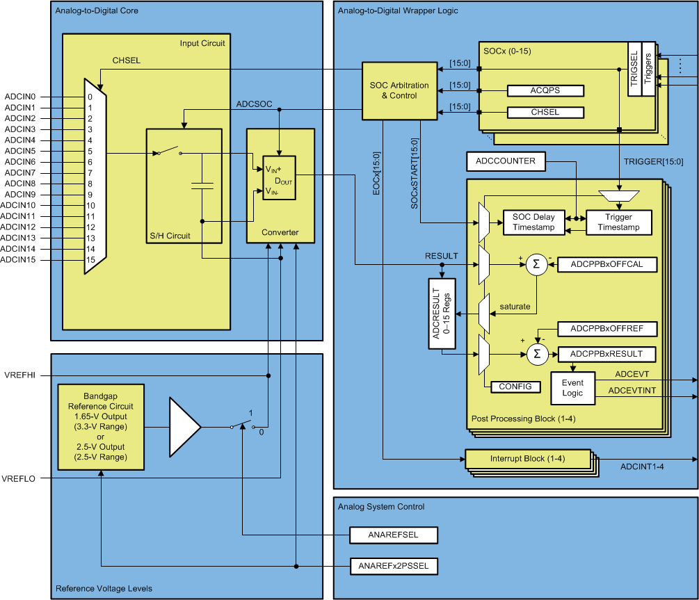
The ADC module described here is a successive approximation (SAR) style ADC with resolution of 12 bits. This section refers to the analog circuits of the converter as the “core,” and includes the channel-select MUX, the sample-and-hold (S/H) circuit, the successive approximation circuits, voltage reference circuits, and other analog support circuits. The digital circuits of the converter are referred to as the “wrapper” and include logic for programmable conversions, result registers, interfaces to analog circuits, interfaces to the peripheral buses, post-processing circuits, and interfaces to other on-chip modules.
Each ADC module consists of a single sample-and-hold (S/H) circuit. The ADC module is designed to be duplicated multiple times on the same chip, allowing simultaneous sampling or independent operation of multiple ADCs. The ADC wrapper is start-of-conversion (SOC)-based (see the SOC Principle of Operation section of the Analog-to-Digital Converter (ADC) chapter in the TMS320F28003x Real-Time Microcontrollers Technical Reference Manual).
Each ADC has the following features:
- Resolution of 12 bits
- Ratiometric external reference set by VREFHI/VREFLO
- Selectable internal reference of 2.5 V or 3.3 V
- Single-ended signal mode
- Input multiplexer with up to 16 channels
- 16 configurable SOCs
- 16 individually addressable result registers
- Multiple trigger sources
- Software immediate start
- All ePWMs: ADCSOC A or B
- GPIO XINT2
- CPU Timers 0/1/2
- ADCINT1/2
- Four flexible PIE interrupts
- Burst-mode triggering option
- Four post-processing blocks,
each with:
- Saturating offset calibration
- Error from setpoint calculation
- High, low, and zero-crossing compare, with interrupt and ePWM trip capability
- Trigger-to-sample delay capture
The block diagram for the ADC core and ADC wrapper are shown in Figure 6-42.
 Figure 6-42 ADC Module Block
Diagram