SPRSP65G April 2021 – May 2024 AM2431 , AM2432 , AM2434
PRODUCTION DATA
- 1
- 1 Features
- 2 Applications
- 3 Description
- 4 Device Comparison
-
5 Terminal Configuration and Functions
- 5.1 Pin Diagram
- 5.2 Pin Attributes
- 5.3
Signal Descriptions
- 17
- 5.3.1 AM243x_ALX Package - Unsupported Interfaces and Signals
- 5.3.2 ADC
- 5.3.3 CPSW
- 5.3.4 CPTS
- 5.3.5 DDRSS
- 5.3.6 ECAP
- 5.3.7 Emulation and Debug
- 5.3.8 EPWM
- 5.3.9 EQEP
- 5.3.10 FSI
- 5.3.11 GPIO
- 5.3.12 GPMC
- 5.3.13 I2C
- 5.3.14 MCAN
- 5.3.15 SPI (MCSPI)
- 5.3.16 MMC
- 5.3.17 OSPI
- 5.3.18 Power Supply
- 5.3.19 PRU_ICSSG
- 5.3.20 Reserved
- 5.3.21 SERDES
- 5.3.22 System and Miscellaneous
- 5.3.23 TIMER
- 5.3.24 UART
- 5.3.25 USB
- 5.4 Pin Connectivity Requirements
-
6 Specifications
- 6.1 Absolute Maximum Ratings
- 6.2 ESD Ratings
- 6.3 Power-On Hours (POH)
- 6.4 Recommended Operating Conditions
- 6.5 Operating Performance Points
- 6.6 Power Consumption Summary
- 6.7
Electrical Characteristics
- 6.7.1 I2C Open-Drain, and Fail-Safe (I2C OD FS) Electrical Characteristics
- 6.7.2 Fail-Safe Reset (FS RESET) Electrical Characteristics
- 6.7.3 High-Frequency Oscillator (HFOSC) Electrical Characteristics
- 6.7.4 eMMCPHY Electrical Characteristics
- 6.7.5 SDIO Electrical Characteristics
- 6.7.6 LVCMOS Electrical Characteristics
- 6.7.7 ADC12B Electrical Characteristics (ALV package)
- 6.7.8 ADC10B Electrical Characteristics (ALX package)
- 6.7.9 USB2PHY Electrical Characteristics
- 6.7.10 SerDes PHY Electrical Characteristics
- 6.7.11 DDR Electrical Characteristics
- 6.8 VPP Specifications for One-Time Programmable (OTP) eFuses
- 6.9 Thermal Resistance Characteristics
- 6.10
Timing and Switching Characteristics
- 6.10.1 Timing Parameters and Information
- 6.10.2 Power Supply Requirements
- 6.10.3 System Timing
- 6.10.4 Clock Specifications
- 6.10.5
Peripherals
- 6.10.5.1 CPSW3G
- 6.10.5.2 DDRSS
- 6.10.5.3 ECAP
- 6.10.5.4 EPWM
- 6.10.5.5 EQEP
- 6.10.5.6 FSI
- 6.10.5.7 GPIO
- 6.10.5.8 GPMC
- 6.10.5.9 I2C
- 6.10.5.10 MCAN
- 6.10.5.11 MCSPI
- 6.10.5.12 MMCSD
- 6.10.5.13 CPTS
- 6.10.5.14 OSPI
- 6.10.5.15 PCIe
- 6.10.5.16
PRU_ICSSG
- 6.10.5.16.1 PRU_ICSSG Programmable Real-Time Unit (PRU)
- 6.10.5.16.2 PRU_ICSSG Pulse Width Modulation (PWM)
- 6.10.5.16.3 PRU_ICSSG Industrial Ethernet Peripheral (IEP)
- 6.10.5.16.4 PRU_ICSSG Universal Asynchronous Receiver Transmitter (UART)
- 6.10.5.16.5 PRU_ICSSG Enhanced Capture Peripheral (ECAP)
- 6.10.5.16.6 PRU_ICSSG RGMII, MII_RT, and Switch
- 6.10.5.17 Timers
- 6.10.5.18 UART
- 6.10.5.19 USB
- 6.10.6 Emulation and Debug
-
7 Detailed Description
- 7.1 Overview
- 7.2 Processor Subsystems
- 7.3 Accelerators and Coprocessors
- 7.4
Other Subsystems
- 7.4.1 PDMA Controller
- 7.4.2
Peripherals
- 7.4.2.1 ADC
- 7.4.2.2 DCC
- 7.4.2.3 Dual Date Rate (DDR) External Memory Interface (DDRSS)
- 7.4.2.4 ECAP
- 7.4.2.5 EPWM
- 7.4.2.6 ELM
- 7.4.2.7 ESM
- 7.4.2.8 GPIO
- 7.4.2.9 EQEP
- 7.4.2.10 General-Purpose Memory Controller (GPMC)
- 7.4.2.11 I2C
- 7.4.2.12 MCAN
- 7.4.2.13 MCRC Controller
- 7.4.2.14 MCSPI
- 7.4.2.15 MMCSD
- 7.4.2.16 OSPI
- 7.4.2.17 Peripheral Component Interconnect Express (PCIe)
- 7.4.2.18 Serializer/Deserializer (SerDes) PHY
- 7.4.2.19 Real Time Interrupt (RTI/WWDT)
- 7.4.2.20 Dual Mode Timer (DMTIMER)
- 7.4.2.21 UART
- 7.4.2.22 Universal Serial Bus Subsystem (USBSS)
-
8 Applications,
Implementation, and Layout
- 8.1 Device Connection and Layout Fundamentals
- 8.2
Peripheral- and Interface-Specific Design Information
- 8.2.1 General Routing Guidelines
- 8.2.2 DDR Board Design and Layout Guidelines
- 8.2.3 OSPI/QSPI/SPI Board Design and Layout Guidelines
- 8.2.4 USB VBUS Design Guidelines
- 8.2.5 System Power Supply Monitor Design Guidelines
- 8.2.6 High Speed Differential Signal Routing Guidance
- 8.2.7 Thermal Solution Guidance
- 8.3 Clock Routing Guidelines
- 9 Device and Documentation Support
- 10Revision History
- 11Mechanical, Packaging, and Orderable Information
6.10.4.1.1 MCU_OSC0 Internal Oscillator Clock Source
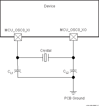
Figure 6-15 shows the recommended crystal circuit. All discrete components used to implement the oscillator circuit must be placed as close as possible to the MCU_OSC0_XI and MCU_OSC0_XO pins.
 Figure 6-15 MCU_OSC0
Crystal Implementation
Figure 6-15 MCU_OSC0
Crystal ImplementationThe crystal must be in the fundamental mode of operation and parallel resonant. Table 6-19 summarizes the required electrical constraints.
Table 6-19 MCU_OSC0 Crystal Circuit Requirements
| PARAMETER | MIN | TYP | MAX | UNIT | |||
|---|---|---|---|---|---|---|---|
| Fxtal | Crystal Parallel Resonance Frequency | 25 | MHz | ||||
| Fxtal | Crystal Frequency Stability and Tolerance | Ethernet RGMII and RMII not used | ±100 | ppm | |||
| Ethernet RGMII and RMII using derived clock | ±50 | ||||||
| CL1+PCBXI | Capacitance of CL1 + CPCBXI | 12 | 24 | pF | |||
| CL2+PCBXO | Capacitance of CL2 + CPCBXO | 12 | 24 | pF | |||
| CL | Crystal Load Capacitance | 6 | 12 | pF | |||
| Cshunt | Crystal Circuit Shunt Capacitance | ESRxtal = 30 Ω | 25MHz | 7 | pF | ||
| ESRxtal = 40 Ω | 25MHz | 5 | pF | ||||
| ESRxtal = 50 Ω | 25MHz | 5 | pF | ||||
| ESRxtal | Crystal Effective Series Resistance | (1) | Ω | ||||
(1) The maximum ESR of the crystal is a function of the crystal frequency and shunt capacitance. See the Cshunt parameter.
When selecting a crystal, the system design must consider temperature and aging characteristics of the crystal based on worst case environment and expected life expectancy of the system.
Table 6-20 details the switching characteristics of the oscillator.
Table 6-20 MCU_OSC0
Switching Characteristics - Crystal Mode
| PARAMETER | MIN | TYP | MAX | UNIT | |
|---|---|---|---|---|---|
| CXI | XI Capacitance | 1.44 | pF | ||
| CXO | XO Capacitance | 1.52 | pF | ||
| CXIXO | XI to XO Mutual Capacitance | 0.01 | pF | ||
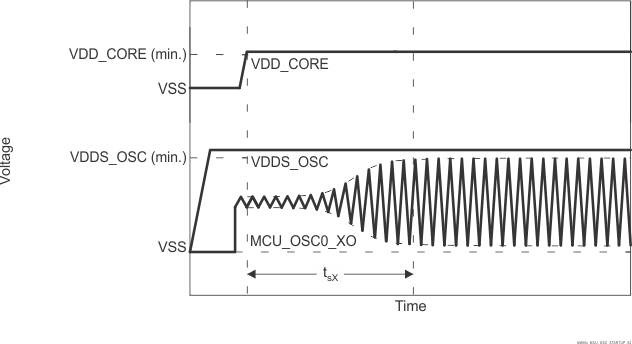
| ts | Start-up Time | 4 | ms | ||
 Figure 6-16 MCU_OSC0 Start-up Time