SPRSP85A April   2024  – September 2024 TMS320F28P550SJ , TMS320F28P559SJ-Q1

PRODMIX  

  1.   1
  2. Features
  3. Applications
  4. Description
    1. 3.1 Functional Block Diagram
  5. Device Comparison
    1. 4.1 Related Products
  6. Pin Configuration and Functions
    1. 5.1 Pin Diagrams
    2. 5.2 Pin Attributes
    3. 5.3 Signal Descriptions
      1. 5.3.1 Analog Signals
      2. 5.3.2 Digital Signals
      3. 5.3.3 Power and Ground
      4. 5.3.4 Test, JTAG, and Reset
    4. 5.4 Pin Multiplexing
      1. 5.4.1 GPIO Muxed Pins
      2. 5.4.2 Digital Inputs on ADC Pins (AIOs)
      3. 5.4.3 Digital Inputs and Outputs on ADC Pins (AGPIOs)
      4. 5.4.4 GPIO Input X-BAR
      5. 5.4.5 GPIO Output X-BAR, CLB X-BAR, CLB Output X-BAR, and ePWM X-BAR
    5. 5.5 Pins With Internal Pullup and Pulldown
    6. 5.6 Connections for Unused Pins
  7. Specifications
    1. 6.1  Absolute Maximum Ratings
    2. 6.2  ESD Ratings – Commercial
    3. 6.3  ESD Ratings – Automotive
    4. 6.4  Recommended Operating Conditions
    5. 6.5  Power Consumption Summary
      1. 6.5.1 System Current Consumption - VREG Enable - Internal Supply
      2. 6.5.2 System Current Consumption - VREG Disable - External Supply
      3. 6.5.3 Operating Mode Test Description
      4. 6.5.4 Reducing Current Consumption
        1. 6.5.4.1 Typical Current Reduction per Disabled Peripheral
    6. 6.6  Electrical Characteristics
    7. 6.7  Special Considerations for 5V Fail-Safe Pins
    8. 6.8  Thermal Resistance Characteristics for PDT Package
    9. 6.9  Thermal Resistance Characteristics for PZ Package
    10. 6.10 Thermal Resistance Characteristics for PNA Package
    11. 6.11 Thermal Resistance Characteristics for PM Package
    12. 6.12 Thermal Resistance Characteristics for RSH Package
    13. 6.13 Thermal Design Considerations
    14. 6.14 System
      1. 6.14.1  Power Management Module (PMM)
        1. 6.14.1.1 Introduction
        2. 6.14.1.2 Overview
          1. 6.14.1.2.1 Power Rail Monitors
            1. 6.14.1.2.1.1 I/O POR (Power-On Reset) Monitor
            2. 6.14.1.2.1.2 I/O BOR (Brown-Out Reset) Monitor
            3. 6.14.1.2.1.3 VDD POR (Power-On Reset) Monitor
          2. 6.14.1.2.2 External Supervisor Usage
          3. 6.14.1.2.3 Delay Blocks
          4. 6.14.1.2.4 Internal 1.2-V LDO Voltage Regulator (VREG)
          5. 6.14.1.2.5 VREGENZ
        3. 6.14.1.3 External Components
          1. 6.14.1.3.1 Decoupling Capacitors
            1. 6.14.1.3.1.1 VDDIO Decoupling
            2. 6.14.1.3.1.2 VDD Decoupling
        4. 6.14.1.4 Power Sequencing
          1. 6.14.1.4.1 Supply Pins Ganging
          2. 6.14.1.4.2 Signal Pins Power Sequence
          3. 6.14.1.4.3 Supply Pins Power Sequence
            1. 6.14.1.4.3.1 External VREG/VDD Mode Sequence
            2. 6.14.1.4.3.2 Internal VREG/VDD Mode Sequence
            3. 6.14.1.4.3.3 Supply Sequencing Summary and Effects of Violations
            4. 6.14.1.4.3.4 Supply Slew Rate
        5. 6.14.1.5 Power Management Module Electrical Data and Timing
          1. 6.14.1.5.1 Power Management Module Operating Conditions
          2. 6.14.1.5.2 Power Management Module Characteristics
      2. 6.14.2  Reset Timing
        1. 6.14.2.1 Reset Sources
        2. 6.14.2.2 Reset Electrical Data and Timing
          1. 6.14.2.2.1 Reset - XRSn - Timing Requirements
          2. 6.14.2.2.2 Reset - XRSn - Switching Characteristics
          3. 6.14.2.2.3 Reset Timing Diagrams
      3. 6.14.3  Clock Specifications
        1. 6.14.3.1 Clock Sources
        2. 6.14.3.2 Clock Frequencies, Requirements, and Characteristics
          1. 6.14.3.2.1 Input Clock Frequency and Timing Requirements, PLL Lock Times
            1. 6.14.3.2.1.1 Input Clock Frequency
            2. 6.14.3.2.1.2 XTAL Oscillator Characteristics
            3. 6.14.3.2.1.3 X1 Input Level Characteristics When Using an External Clock Source - Not a Crystal
            4. 6.14.3.2.1.4 X1 Timing Requirements
            5. 6.14.3.2.1.5 AUXCLKIN Timing Requirements
            6. 6.14.3.2.1.6 APLL Characteristics
            7. 6.14.3.2.1.7 XCLKOUT Switching Characteristics - PLL Bypassed or Enabled
            8. 6.14.3.2.1.8 Internal Clock Frequencies
        3. 6.14.3.3 Input Clocks and PLLs
        4. 6.14.3.4 XTAL Oscillator
          1. 6.14.3.4.1 Introduction
          2. 6.14.3.4.2 Overview
            1. 6.14.3.4.2.1 Electrical Oscillator
              1. 6.14.3.4.2.1.1 Modes of Operation
                1. 6.14.3.4.2.1.1.1 Crystal Mode of Operation
                2. 6.14.3.4.2.1.1.2 Single-Ended Mode of Operation
              2. 6.14.3.4.2.1.2 XTAL Output on XCLKOUT
            2. 6.14.3.4.2.2 Quartz Crystal
            3. 6.14.3.4.2.3 GPIO Modes of Operation
          3. 6.14.3.4.3 Functional Operation
            1. 6.14.3.4.3.1 ESR – Effective Series Resistance
            2. 6.14.3.4.3.2 Rneg – Negative Resistance
            3. 6.14.3.4.3.3 Start-up Time
              1. 6.14.3.4.3.3.1 X1/X2 Precondition
            4. 6.14.3.4.3.4 DL – Drive Level
          4. 6.14.3.4.4 How to Choose a Crystal
          5. 6.14.3.4.5 Testing
          6. 6.14.3.4.6 Common Problems and Debug Tips
          7. 6.14.3.4.7 Crystal Oscillator Specifications
            1. 6.14.3.4.7.1 Crystal Oscillator Electrical Characteristics
            2. 6.14.3.4.7.2 Crystal Equivalent Series Resistance (ESR) Requirements
            3. 6.14.3.4.7.3 Crystal Oscillator Parameters
        5. 6.14.3.5 Internal Oscillators
          1. 6.14.3.5.1 INTOSC Characteristics
      4. 6.14.4  Flash Parameters
        1. 6.14.4.1 Flash Parameters 
      5. 6.14.5  RAM Specifications
      6. 6.14.6  ROM Specifications
      7. 6.14.7  Emulation/JTAG
        1. 6.14.7.1 JTAG Electrical Data and Timing
          1. 6.14.7.1.1 JTAG Timing Requirements
          2. 6.14.7.1.2 JTAG Switching Characteristics
          3. 6.14.7.1.3 JTAG Timing Diagram
        2. 6.14.7.2 cJTAG Electrical Data and Timing
          1. 6.14.7.2.1 cJTAG Timing Requirements
          2. 6.14.7.2.2 cJTAG Switching Characteristics
          3. 6.14.7.2.3 cJTAG Timing Diagram
      8. 6.14.8  GPIO Electrical Data and Timing
        1. 6.14.8.1 GPIO – Output Timing
          1. 6.14.8.1.1 General-Purpose Output Switching Characteristics
          2. 6.14.8.1.2 General-Purpose Output Timing Diagram
        2. 6.14.8.2 GPIO – Input Timing
          1. 6.14.8.2.1 General-Purpose Input Timing Requirements
          2. 6.14.8.2.2 Sampling Mode
        3. 6.14.8.3 Sampling Window Width for Input Signals
      9. 6.14.9  Interrupts
        1. 6.14.9.1 External Interrupt (XINT) Electrical Data and Timing
          1. 6.14.9.1.1 External Interrupt Timing Requirements
          2. 6.14.9.1.2 External Interrupt Switching Characteristics
          3. 6.14.9.1.3 External Interrupt Timing
      10. 6.14.10 Low-Power Modes
        1. 6.14.10.1 Clock-Gating Low-Power Modes
        2. 6.14.10.2 Low-Power Mode Wake-up Timing
          1. 6.14.10.2.1 IDLE Mode Timing Requirements
          2. 6.14.10.2.2 IDLE Mode Switching Characteristics
          3. 6.14.10.2.3 IDLE Entry and Exit Timing Diagram
          4. 6.14.10.2.4 STANDBY Mode Timing Requirements
          5. 6.14.10.2.5 STANDBY Mode Switching Characteristics
          6. 6.14.10.2.6 STANDBY Entry and Exit Timing Diagram
          7. 6.14.10.2.7 HALT Mode Timing Requirements
          8. 6.14.10.2.8 HALT Mode Switching Characteristics
          9. 6.14.10.2.9 HALT Entry and Exit Timing Diagram
    15. 6.15 Analog Peripherals
      1. 6.15.1 Block Diagram
      2. 6.15.2 Analog Pins and Internal Connections
      3. 6.15.3 Analog Signal Descriptions
      4. 6.15.4 Analog-to-Digital Converter (ADC)
        1. 6.15.4.1 ADC Configurability
          1. 6.15.4.1.1 Signal Mode
        2. 6.15.4.2 ADC Electrical Data and Timing
          1. 6.15.4.2.1 ADC Operating Conditions
          2. 6.15.4.2.2 ADC Characteristics
          3. 6.15.4.2.3 ADC INL and DNL
          4. 6.15.4.2.4 ADC Performance Per Pin
          5. 6.15.4.2.5 ADC Input Model
          6. 6.15.4.2.6 ADC Timing Diagrams
      5. 6.15.5 Temperature Sensor
        1. 6.15.5.1 Temperature Sensor Electrical Data and Timing
          1. 6.15.5.1.1 Temperature Sensor Characteristics
      6. 6.15.6 Comparator Subsystem (CMPSS)
        1. 6.15.6.1 CMPx_DACL
        2. 6.15.6.2 CMPSS Connectivity Diagram
        3. 6.15.6.3 Block Diagram
        4. 6.15.6.4 CMPSS Electrical Data and Timing
          1. 6.15.6.4.1 CMPSS Comparator Electrical Characteristics
          2.        CMPSS Comparator Input Referred Offset and Hysteresis
          3. 6.15.6.4.2 CMPSS DAC Static Electrical Characteristics
          4. 6.15.6.4.3 CMPSS Illustrative Graphs
          5. 6.15.6.4.4 Buffered Output from CMPx_DACL Operating Conditions
          6. 6.15.6.4.5 Buffered Output from CMPx_DACL Electrical Characteristics
      7. 6.15.7 Buffered Digital-to-Analog Converter (DAC)
        1. 6.15.7.1 Buffered DAC Electrical Data and Timing
          1. 6.15.7.1.1 Buffered DAC Operating Conditions
          2. 6.15.7.1.2 Buffered DAC Electrical Characteristics
      8. 6.15.8 Programmable Gain Amplifier (PGA)
        1. 6.15.8.1 PGA Electrical Data and Timing
          1. 6.15.8.1.1 PGA Operating Conditions
          2. 6.15.8.1.2 PGA Characteristics
    16. 6.16 Control Peripherals
      1. 6.16.1 Enhanced Pulse Width Modulator (ePWM)
        1. 6.16.1.1 Control Peripherals Synchronization
        2. 6.16.1.2 ePWM Electrical Data and Timing
          1. 6.16.1.2.1 ePWM Timing Requirements
          2. 6.16.1.2.2 ePWM Switching Characteristics
          3. 6.16.1.2.3 Trip-Zone Input Timing
            1. 6.16.1.2.3.1 Trip-Zone Input Timing Requirements
            2. 6.16.1.2.3.2 PWM Hi-Z Characteristics Timing Diagram
      2. 6.16.2 High-Resolution Pulse Width Modulator (HRPWM)
        1. 6.16.2.1 HRPWM Electrical Data and Timing
          1. 6.16.2.1.1 High-Resolution PWM Characteristics
      3. 6.16.3 External ADC Start-of-Conversion Electrical Data and Timing
        1. 6.16.3.1 External ADC Start-of-Conversion Switching Characteristics
        2. 6.16.3.2 ADCSOCAO or ADCSOCBO Timing Diagram
      4. 6.16.4 Enhanced Capture (eCAP)
        1. 6.16.4.1 eCAP Block Diagram
        2. 6.16.4.2 eCAP Synchronization
        3. 6.16.4.3 eCAP Electrical Data and Timing
          1. 6.16.4.3.1 eCAP Timing Requirements
          2. 6.16.4.3.2 eCAP Switching Characteristics
      5. 6.16.5 Enhanced Quadrature Encoder Pulse (eQEP)
        1. 6.16.5.1 eQEP Electrical Data and Timing
          1. 6.16.5.1.1 eQEP Timing Requirements
          2. 6.16.5.1.2 eQEP Switching Characteristics
    17. 6.17 Communications Peripherals
      1. 6.17.1 Modular Controller Area Network (MCAN)
      2. 6.17.2 Inter-Integrated Circuit (I2C)
        1. 6.17.2.1 I2C Electrical Data and Timing
          1. 6.17.2.1.1 I2C Timing Requirements
          2. 6.17.2.1.2 I2C Switching Characteristics
          3. 6.17.2.1.3 I2C Timing Diagram
      3. 6.17.3 Power Management Bus (PMBus) Interface
        1. 6.17.3.1 PMBus Electrical Data and Timing
          1. 6.17.3.1.1 PMBus Electrical Characteristics
          2. 6.17.3.1.2 PMBus Fast Plus Mode Switching Characteristics
          3. 6.17.3.1.3 PMBus Fast Mode Switching Characteristics
          4. 6.17.3.1.4 PMBus Standard Mode Switching Characteristics
      4. 6.17.4 Serial Communications Interface (SCI)
      5. 6.17.5 Serial Peripheral Interface (SPI)
        1. 6.17.5.1 SPI Controller Mode Timings
          1. 6.17.5.1.1 SPI Controller Mode Timing Requirements
          2. 6.17.5.1.2 SPI Controller Mode Switching Characteristics - Clock Phase 0
          3. 6.17.5.1.3 SPI Controller Mode Switching Characteristics - Clock Phase 1
          4. 6.17.5.1.4 SPI Controller Mode Timing Diagrams
        2. 6.17.5.2 SPI Peripheral Mode Timings
          1. 6.17.5.2.1 SPI Peripheral Mode Timing Requirements
          2. 6.17.5.2.2 SPI Peripheral Mode Switching Characteristics
          3. 6.17.5.2.3 SPI Peripheral Mode Timing Diagrams
      6. 6.17.6 Local Interconnect Network (LIN)
      7. 6.17.7 Fast Serial Interface (FSI)
        1. 6.17.7.1 FSI Transmitter
          1. 6.17.7.1.1 FSITX Electrical Data and Timing
            1. 6.17.7.1.1.1 FSITX Switching Characteristics
            2. 6.17.7.1.1.2 FSITX Timings
        2. 6.17.7.2 FSI Receiver
          1. 6.17.7.2.1 FSIRX Electrical Data and Timing
            1. 6.17.7.2.1.1 FSIRX Timing Requirements
            2. 6.17.7.2.1.2 FSIRX Switching Characteristics
            3. 6.17.7.2.1.3 FSIRX Timings
        3. 6.17.7.3 FSI SPI Compatibility Mode
          1. 6.17.7.3.1 FSITX SPI Signaling Mode Electrical Data and Timing
            1. 6.17.7.3.1.1 FSITX SPI Signaling Mode Switching Characteristics
            2. 6.17.7.3.1.2 FSITX SPI Signaling Mode Timings
      8. 6.17.8 Universal Serial Bus (USB)
        1. 6.17.8.1 USB Electrical Data and Timing
          1. 6.17.8.1.1 USB Input Ports DP and DM Timing Requirements
          2. 6.17.8.1.2 USB Output Ports DP and DM Switching Characteristics
  8. Detailed Description
    1. 7.1  Overview
    2. 7.2  Functional Block Diagram
    3. 7.3  Memory
      1. 7.3.1 Memory Map
        1. 7.3.1.1 Dedicated RAM (Mx RAM)
        2. 7.3.1.2 Local Shared RAM (LSx RAM)
        3. 7.3.1.3 Global Shared RAM (GSx RAM)
        4. 7.3.1.4 Message RAM
      2. 7.3.2 Control Law Accelerator (CLA) Memory Map
      3. 7.3.3 Flash Memory Map
        1. 7.3.3.1 Addresses of Flash Sectors
      4. 7.3.4 Peripheral Registers Memory Map
    4. 7.4  Identification
    5. 7.5  Bus Architecture – Peripheral Connectivity
    6. 7.6  C28x Processor
      1. 7.6.1 Floating-Point Unit (FPU)
      2. 7.6.2 Trigonometric Math Unit (TMU)
      3. 7.6.3 VCRC Unit
    7. 7.7  Control Law Accelerator (CLA)
    8. 7.8  Embedded Real-Time Analysis and Diagnostic (ERAD)
    9. 7.9  Direct Memory Access (DMA)
    10. 7.10 Device Boot Modes
      1. 7.10.1 Device Boot Configurations
        1. 7.10.1.1 Configuring Boot Mode Pins
        2. 7.10.1.2 Configuring Boot Mode Table Options
      2. 7.10.2 GPIO Assignments
    11. 7.11 Security
      1. 7.11.1 Securing the Boundary of the Chip
        1. 7.11.1.1 JTAGLOCK
        2. 7.11.1.2 Zero-pin Boot
      2. 7.11.2 Dual-Zone Security
      3. 7.11.3 Disclaimer
    12. 7.12 Watchdog
    13. 7.13 C28x Timers
    14. 7.14 Dual-Clock Comparator (DCC)
      1. 7.14.1 Features
      2. 7.14.2 Mapping of DCCx Clock Source Inputs
    15. 7.15 Configurable Logic Block (CLB)
  9. Reference Design
  10. Device and Documentation Support
    1. 9.1 Device Nomenclature
    2. 9.2 Markings
    3. 9.3 Tools and Software
    4. 9.4 Documentation Support
    5. 9.5 Support Resources
    6. 9.6 Trademarks
    7. 9.7 Electrostatic Discharge Caution
    8. 9.8 Glossary
  11. 10Revision History
  12. 11Mechanical, Packaging, and Orderable Information
    1. 11.1 Package Option Addendum
    2.     TAPE AND REEL INFORMATION
    3.     TRAY

Modular Controller Area Network (MCAN)

The Controller Area Network (CAN) is a serial communications protocol that efficiently supports distributed real-time control with a high level of reliability. CAN has high immunity to electrical interference and the ability to detect various type of errors. In CAN, many short messages are broadcast to the entire network, which provides data consistency in every node of the system.

The MCAN module supports both classic CAN and CAN FD (CAN with flexible data-rate) protocols. The CAN FD feature allows higher throughput and increased payload per data frame. Classic CAN and CAN FD devices may coexist on the same network without any conflict provided that partial network transceivers, which can detect and ignore CAN FD without generating bus errors, are used by the classic CAN devices. The MCAN module is compliant to ISO 11898-1:2015.

Note:

The availability of the CAN FD feature is dependent on the device's part number. Refer to the device data sheet for more information.
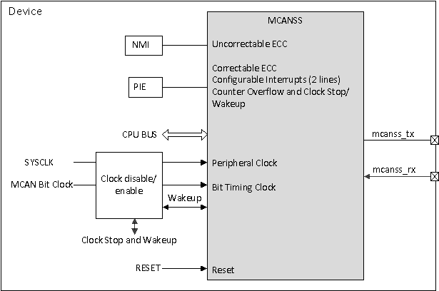
TMS320F28P550SJ TMS320F28P559SJ-Q1 MCAN Module Overview Figure 6-64 MCAN Module Overview

The MCAN module implements the following features:

  • Conforms with CAN Protocol 2.0 A, B and ISO 11898-1:2015
  • Full CAN FD support (up to 64 data bytes)
  • AUTOSAR and SAE J1939 support
  • Flexible Message RAM allocation (maximum configuration below is for a device with 4352 32-bit word message RAM)
    • Up to 32 dedicated transmit buffers
    • Configurable transmit FIFO, up to 32 elements
    • Configurable transmit queue, up to 32 elements
    • Configurable transmit Event FIFO, up to 32 elements
    • Up to 64 dedicated receive buffers
    • Two configurable receive FIFOs, up to 64 elements each
    • Up to 128 filter elements
  • Loop-back mode for self-test
  • Maskable interrupt (two configurable interrupt lines, correctable ECC, counter overflow and clock stop/wakeup)
  • Non-maskable interrupt (uncorrectable ECC)
  • Two clock domains (CAN clock/host clock)
  • ECC check for Message RAM
  • Clock stop and wake-up support
  • Timestamp counter

Non-supported features:

  • Host bus firewall
  • Clock calibration
  • Debug over CAN