SPRSP96A March   2024  – September 2024 TDA4AEN-Q1 , TDA4VEN-Q1

PRODUCTION DATA  

  1.   1
  2. Features
  3. Applications
  4. Description
    1. 3.1 Functional Block Diagram
  5. Device Comparison
  6. Terminal Configuration and Functions
    1. 5.1 Pin Diagrams
    2. 5.2 Pin Attributes
      1.      10
      2.      11
    3. 5.3 Signal Descriptions
      1.      13
      2. 5.3.1  CPSW3G
        1. 5.3.1.1 MAIN Domain
          1.        16
          2.        17
          3.        18
          4.        19
      3. 5.3.2  CPTS
        1. 5.3.2.1 MAIN Domain
          1.        22
      4. 5.3.3  CSI-2
        1. 5.3.3.1 MAIN Domain
          1.        25
          2.        26
          3.        27
          4.        28
      5. 5.3.4  DDRSS
        1. 5.3.4.1 MAIN Domain
          1.        31
      6. 5.3.5  DSI
        1. 5.3.5.1 MAIN Domain
          1.        34
      7. 5.3.6  DSS
        1. 5.3.6.1 MAIN Domain
          1.        37
      8. 5.3.7  ECAP
        1. 5.3.7.1 MAIN Domain
          1.        40
          2.        41
          3.        42
      9. 5.3.8  Emulation and Debug
        1. 5.3.8.1 MAIN Domain
          1.        45
        2. 5.3.8.2 MCU Domain
          1.        47
      10. 5.3.9  EPWM
        1. 5.3.9.1 MAIN Domain
          1.        50
          2.        51
          3.        52
          4.        53
      11. 5.3.10 EQEP
        1. 5.3.10.1 MAIN Domain
          1.        56
          2.        57
          3.        58
      12. 5.3.11 GPIO
        1. 5.3.11.1 MAIN Domain
          1.        61
          2.        62
        2. 5.3.11.2 MCU Domain
          1.        64
      13. 5.3.12 GPMC
        1. 5.3.12.1 MAIN Domain
          1.        67
      14. 5.3.13 I2C
        1. 5.3.13.1 MAIN Domain
          1.        70
          2.        71
          3.        72
          4.        73
          5.        74
        2. 5.3.13.2 MCU Domain
          1.        76
        3. 5.3.13.3 WKUP Domain
          1.        78
      15. 5.3.14 MCAN
        1. 5.3.14.1 MAIN Domain
          1.        81
          2.        82
        2. 5.3.14.2 MCU Domain
          1.        84
          2.        85
      16. 5.3.15 MCASP
        1. 5.3.15.1 MAIN Domain
          1.        88
          2.        89
          3.        90
          4.        91
          5.        92
      17. 5.3.16 MCSPI
        1. 5.3.16.1 MAIN Domain
          1.        95
          2.        96
          3.        97
        2. 5.3.16.2 MCU Domain
          1.        99
          2.        100
      18. 5.3.17 MDIO
        1. 5.3.17.1 MAIN Domain
          1.        103
      19. 5.3.18 MMC
        1. 5.3.18.1 MAIN Domain
          1.        106
          2.        107
          3.        108
      20. 5.3.19 OLDI
        1. 5.3.19.1 MAIN Domain
          1.        111
      21. 5.3.20 OSPI
        1. 5.3.20.1 MAIN Domain
          1.        114
      22. 5.3.21 Power Supply
        1.       116
      23. 5.3.22 Reserved
        1.       118
      24. 5.3.23 SERDES
        1. 5.3.23.1 MAIN Domain
          1.        121
          2.        122
          3.        123
      25. 5.3.24 System and Miscellaneous
        1. 5.3.24.1 Boot Mode Configuration
          1. 5.3.24.1.1 MAIN Domain
            1.         127
        2. 5.3.24.2 Clock
          1. 5.3.24.2.1 MCU Domain
            1.         130
          2. 5.3.24.2.2 WKUP Domain
            1.         132
        3. 5.3.24.3 System
          1. 5.3.24.3.1 MAIN Domain
            1.         135
          2. 5.3.24.3.2 MCU Domain
            1.         137
          3. 5.3.24.3.3 WKUP Domain
            1.         139
        4. 5.3.24.4 VMON
          1.        141
      26. 5.3.25 TIMER
        1. 5.3.25.1 MAIN Domain
          1.        144
        2. 5.3.25.2 MCU Domain
          1.        146
        3. 5.3.25.3 WKUP Domain
          1.        148
      27. 5.3.26 UART
        1. 5.3.26.1 MAIN Domain
          1.        151
          2.        152
          3.        153
          4.        154
          5.        155
          6.        156
          7.        157
        2. 5.3.26.2 MCU Domain
          1.        159
        3. 5.3.26.3 WKUP Domain
          1.        161
      28. 5.3.27 USB
        1. 5.3.27.1 MAIN Domain
          1.        164
          2.        165
    4. 5.4 Pin Connectivity Requirements
  7. Specifications
    1. 6.1 Absolute Maximum Ratings
    2. 6.2 ESD Ratings for AEC - Q100 Qualified Devices in the AMW Package
    3. 6.3 Power-On Hours (POH)
    4. 6.4 Recommended Operating Conditions
    5. 6.5 Operating Performance Points
    6. 6.6 Electrical Characteristics
      1. 6.6.1 I2C Open-Drain, and Fail-Safe (I2C OD FS) Electrical Characteristics
      2. 6.6.2 Fail-Safe Reset (FS RESET) Electrical Characteristics
      3. 6.6.3 High-Frequency Oscillator (HFOSC) Electrical Characteristics
      4. 6.6.4 Low-Frequency Oscillator (LFXOSC) Electrical Characteristics
      5. 6.6.5 SDIO Electrical Characteristics
      6. 6.6.6 LVCMOS Electrical Characteristics
      7. 6.6.7 CSI-2 (D-PHY) Electrical Characteristics
      8. 6.6.8 USB2PHY Electrical Characteristics
      9. 6.6.9 DDR Electrical Characteristics
    7. 6.7 VPP Specifications for One-Time Programmable (OTP) eFuses
      1. 6.7.1 Recommended Operating Conditions for OTP eFuse Programming
      2. 6.7.2 Hardware Requirements
      3. 6.7.3 Programming Sequence
      4. 6.7.4 Impact to Your Hardware Warranty
    8. 6.8 Thermal Resistance Characteristics
      1. 6.8.1 Thermal Resistance Characteristics for AMW Package TBD
    9. 6.9 Timing and Switching Characteristics
      1. 6.9.1 Timing Parameters and Information
      2. 6.9.2 Power Supply Requirements
        1. 6.9.2.1 Power Supply Slew Rate Requirement
        2. 6.9.2.2 Power Supply Sequencing
          1. 6.9.2.2.1 Power-Up Sequencing
          2. 6.9.2.2.2 Power-Down Sequencing
          3. 6.9.2.2.3 Partial IO Power Sequencing
      3. 6.9.3 System Timing
        1. 6.9.3.1 Reset Timing
        2. 6.9.3.2 Error Signal Timing
        3. 6.9.3.3 Clock Timing
      4. 6.9.4 Clock Specifications
        1. 6.9.4.1 Input Clocks / Oscillators
          1. 6.9.4.1.1 MCU_OSC0 Internal Oscillator Clock Source
            1. 6.9.4.1.1.1 Load Capacitance
            2. 6.9.4.1.1.2 Shunt Capacitance
          2. 6.9.4.1.2 MCU_OSC0 LVCMOS Digital Clock Source
          3. 6.9.4.1.3 WKUP_LFOSC0 Internal Oscillator Clock Source
          4. 6.9.4.1.4 WKUP_LFOSC0 LVCMOS Digital Clock Source
          5. 6.9.4.1.5 WKUP_LFOSC0 Not Used
        2. 6.9.4.2 Output Clocks
        3. 6.9.4.3 PLLs
        4. 6.9.4.4 Recommended System Precautions for Clock and Control Signal Transitions
      5. 6.9.5 Peripherals
        1. 6.9.5.1  ATL
          1. 6.9.5.1.1 ATL_PCLK Timing Requirements
          2. 6.9.5.1.2 ATL_AWS[x] Timing Requirements
          3. 6.9.5.1.3 ATL_BWS[x] Timing Requirements
          4. 6.9.5.1.4 ATCLK[x] Switching Characteristics
        2. 6.9.5.2  CPSW3G
          1. 6.9.5.2.1 CPSW3G MDIO Timing
          2. 6.9.5.2.2 CPSW3G RMII Timing
          3. 6.9.5.2.3 CPSW3G RGMII Timing
        3. 6.9.5.3  CPTS
        4. 6.9.5.4  CSI-2
        5. 6.9.5.5  CSI-2 TX
        6. 6.9.5.6  DDRSS
        7. 6.9.5.7  DSS
        8. 6.9.5.8  ECAP
        9. 6.9.5.9  Emulation and Debug
          1. 6.9.5.9.1 Trace
          2. 6.9.5.9.2 JTAG
        10. 6.9.5.10 EPWM
        11. 6.9.5.11 EQEP
        12. 6.9.5.12 GPIO
        13. 6.9.5.13 GPMC
          1. 6.9.5.13.1 GPMC and NOR Flash — Synchronous Mode
          2. 6.9.5.13.2 GPMC and NOR Flash — Asynchronous Mode
          3. 6.9.5.13.3 GPMC and NAND Flash — Asynchronous Mode
        14. 6.9.5.14 I2C
        15. 6.9.5.15 MCAN
        16. 6.9.5.16 MCASP
        17. 6.9.5.17 MCSPI
          1. 6.9.5.17.1 MCSPI — Controller Mode
          2. 6.9.5.17.2 MCSPI — Peripheral Mode
        18. 6.9.5.18 MMCSD
          1. 6.9.5.18.1 MMC0 - eMMC Interface
            1. 6.9.5.18.1.1  Legacy SDR Mode
            2. 6.9.5.18.1.2  High Speed SDR Mode
            3. 6.9.5.18.1.3  High Speed DDR Mode
            4. 6.9.5.18.1.4  HS200 Mode
            5. 6.9.5.18.1.5  HS400 Mode
            6. 6.9.5.18.1.6  UHS–I SDR12 Mode
            7. 6.9.5.18.1.7  UHS–I SDR25 Mode
            8. 6.9.5.18.1.8  UHS–I SDR50 Mode
            9. 6.9.5.18.1.9  UHS–I DDR50 Mode
            10. 6.9.5.18.1.10 UHS–I SDR104 Mode
          2. 6.9.5.18.2 MMC1/MMC2 - SD/SDIO Interface
            1. 6.9.5.18.2.1 Default Speed Mode
            2. 6.9.5.18.2.2 High Speed Mode
            3. 6.9.5.18.2.3 UHS–I SDR12 Mode
            4. 6.9.5.18.2.4 UHS–I SDR25 Mode
            5. 6.9.5.18.2.5 UHS–I SDR50 Mode
            6. 6.9.5.18.2.6 UHS–I DDR50 Mode
            7. 6.9.5.18.2.7 UHS–I SDR104 Mode
        19. 6.9.5.19 OSPI
          1. 6.9.5.19.1 OSPI0 PHY Mode
            1. 6.9.5.19.1.1 OSPI0 With PHY Data Training
            2. 6.9.5.19.1.2 OSPI0 Without Data Training
              1. 6.9.5.19.1.2.1 OSPI0 PHY SDR Timing
              2. 6.9.5.19.1.2.2 OSPI0 PHY DDR Timing
          2. 6.9.5.19.2 OSPI0 Tap Mode
            1. 6.9.5.19.2.1 OSPI0 Tap SDR Timing
            2. 6.9.5.19.2.2 OSPI0 Tap DDR Timing
        20. 6.9.5.20 PCIe
        21. 6.9.5.21 Timers
        22. 6.9.5.22 UART
        23. 6.9.5.23 USB
  8. Detailed Description
    1. 7.1 Overview
  9. Applications, Implementation, and Layout
    1. 8.1 Device Connection and Layout Fundamentals
      1. 8.1.1 Power Supply
        1. 8.1.1.1 Power Distribution Network Implementation Guidance
      2. 8.1.2 External Oscillator
      3. 8.1.3 JTAG, EMU, and TRACE
      4. 8.1.4 Unused Pins
    2. 8.2 Peripheral- and Interface-Specific Design Information
      1. 8.2.1 LPDDR4 Board Design and Layout Guidelines
      2. 8.2.2 OSPI/QSPI/SPI Board Design and Layout Guidelines
        1. 8.2.2.1 No Loopback, Internal PHY Loopback, and Internal Pad Loopback
        2. 8.2.2.2 External Board Loopback
        3. 8.2.2.3 DQS (only available in Octal SPI devices)
      3. 8.2.3 USB VBUS Design Guidelines
      4. 8.2.4 System Power Supply Monitor Design Guidelines
      5. 8.2.5 High Speed Differential Signal Routing Guidance
      6. 8.2.6 Thermal Solution Guidance
    3. 8.3 Clock Routing Guidelines
      1. 8.3.1 Oscillator Routing
  10. Device and Documentation Support
    1. 9.1 Device Nomenclature
      1. 9.1.1 Standard Package Symbolization
      2. 9.1.2 Device Naming Convention
    2. 9.2 Tools and Software
    3. 9.3 Documentation Support
    4. 9.4 Support Resources
    5. 9.5 Trademarks
    6. 9.6 Electrostatic Discharge Caution
    7. 9.7 Glossary
  11. 10Revision History
  12. 11Mechanical, Packaging, and Orderable Information
    1. 11.1 Packaging Information

USB VBUS Design Guidelines

The USB 3.1 specification allows the VBUS voltage to be as high as 5.5V for normal operation, and as high as 20V when the Power Delivery addendum is supported. Some automotive applications require a max voltage to be 30V.

The device requires the VBUS signal voltage be scaled down using an external resistor divider (as shown in the Figure 8-4), which limits the voltage applied to the actual device pin (USB0_VBUS). The tolerance of these external resistors should be equal to or less than 1%, and the leakage current of Zener diode at 5V should be less than 100nA.
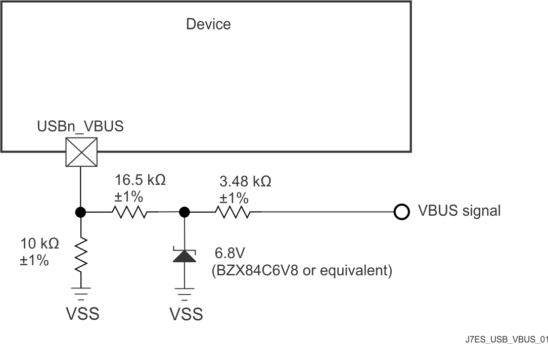
TDA4VEN-Q1 TDA4AEN-Q1 USB VBUS Detect Voltage Divider /
          Clamp Circuit Figure 8-4 USB VBUS Detect Voltage Divider / Clamp Circuit

The USB0_VBUS pin can be considered to be fail-safe because the external circuit in Figure 8-4 limits the input current to the actual device pin in a case where VBUS is applied while the device is powered off.