SPRUIC4D January 2017 – June 2022
5 Hardware References
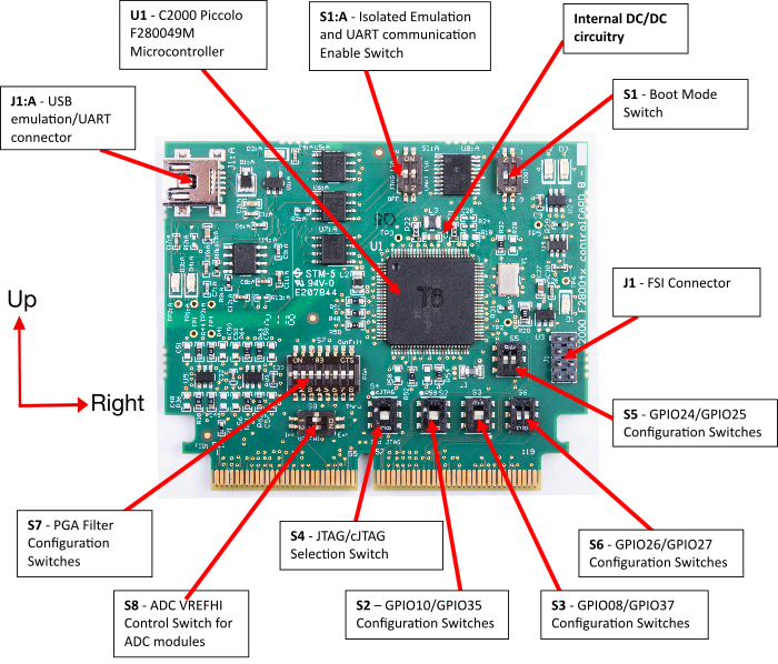
Table 5-1 shows the various connections available on the board. Figure 5-1 illustrates the location of many of these components on the board.
When the controlCARD is used in a high-voltage setup, it is the user’s responsibility to confirm that the voltages and isolation requirements are identified and understood prior to energizing the board or simulation. When energized, the controlCARD or components connected to the controlCARD should not be touched. Furthermore, the capacitor C26:A should be removed to minimize the possibility of leakage current flowing across the isolation barrier of the controlCARD.
 Figure 5-1 Key Components on the controlCARD
| Connectors | |
| J1:A | Emulation/UART connector - USB mini A connector used to provide XDS100v2 emulation and USB-to-UART(SCI) communication through FTDI logic. S1:A determines which connections are enabled to the MCU. |
| Jumpers | |
| J1 | FSI Connector - Gives an ability to connect FSI signals from the F280049C to another board. |
| LEDs | |
| D1 | Turns on when the controlCARD is powered ON (green) |
| D2 | Controlled by GPIO-31 with negative logic (red) |
| D3 | Controlled by GPIO-34 with negative logic (red) |
| D2:A | Turns on when ISO JTAG logic is powered on (green) |
| D3:A | JTAG/UART RX toggle indicator (blue) |
| D4:A | JTAG/UART TX toggle indicator (blue) |
| Resistors and Capacitors (default setting in BOLD) | |
| R18, R19, R21, R22 | GPIO22/23 configuration resistors These resistors allow the user to choose whether GPIO22/23 is used as GPIO (and go to the baseboard) or whether they will be used in conjunction with the F280049C MCU’s internal DC/DC capability:
|
| C19, C20, C21 | These capacitors should be populated when the F280049C’s internal DC/DC capability is used. C19 should be populated with a 2.2-µF capacitor. C20 and C21 should each be populated with a 10-µF capacitor. |
| R24, C28 | R24 and C28 create an optional snubber circuit, which can be used if the DC/DC is used. |
| R36-R47,R49,R53, R60-R64, C41-C47, and C48-C59 | Optional RC input filter for all ADC/PGA inputs |
| C34-C40 | PGA filter capacitor when PGA filtering is used |
| R55-R59 | PGA-GND configuration resistors |
| R48,R50-R52,R54 | These resistors control whether the negative input (PGAGND) for each PGA are grounded locally or whether they should be grounded through pins on the HSEC connector (for use in Kelvin grounding). By default, resistors R55-R59 are not populated and R48, R50-R52, R54 are populated. Because of this, all the PGAs are, by default, expected to be referenced to ground by the baseboard. If, for example, R55 was populated and R48 was unpopulated, then PGA1’s PGAGND would be grounded on the controlCARD. |
| Switches (default position in BOLD) | |
| S1 (Installed with 180 degree rotation) | Boot Mode Selection Switch See Table 5-2 for a list of selectable boot modes. See the device datasheet and TRM for more information about device boot behavior. Left (Switch 2) – GPIO24 Configuration Switch:
Right (Switch 1) – GPIO32 Configuration Switch:
|
| S2 | GPIO10/GPIO35 Configuration Switches
|
| S3 (Installed with 180 degree rotation) | GPIO08/GPIO37 Configuration Switches
|
| S4 | JTAG/cJTAG Selection Switch
|
| S5 (Installed with 180 degree rotation) | GPIO24/GPIO25 Configuration Switches Left (Switch 2) – GPIO25 Configuration Switch:
Right (Switch 1) – GPIO24 Configuration Switch:
|
| S6 | GPIO26/GPIO27 Configuration Switches Left (Switch 1) – GPIO26 Configuration Switch:
Right (Switch 2) – GPIO27 Configuration Switch:
|
| S7 | PGA Filter Configuration Switches From the left, the switches control whether PGA1-PGA7’s outputs, respectively, are filtered. The eighth switch of S7 is not used. Each switch:
The up position for S7’s switch 6 (PGA6) is implemented differently from the other PGAs. PGA6_OF may be accessed through the HSEC connector independently of PGA6_IN, whereas the other PGAs will have their respective PGAn_OF and PGAn_IN signals shorted together. |
| S8 (Installed with 90 degree rotation) | ADC VREFHI Control Switch for ADC modules Top (Switch 1) – VREFHI Control Switch for ADC module A:
Bottom (Switch 2) – VREFHI Control Switch for ADC module B and module C:
|
| S1:A | Isolated emulation and UART communication enable switches Left (Switch 1) – JTAG Enable:
Right (Switch 2) – ISO UART communication enable:
|
| Mode # | GPIO-24 (Left, Switch 2) | GPIO-32 (Right, Switch 1) | Boot from |
|---|---|---|---|
| 00 | 0 (Down) | 0 (Down) | Parallel I/O |
| 01 | 0 (Down) | 1 (Up) | Boot from SCI / Wait Mode |
| 02 | 1 (Up) | 0 (Down) | Boot from CAN |
| 03 | 1 (Up) | 1 (Up) | Boot from FLASH |